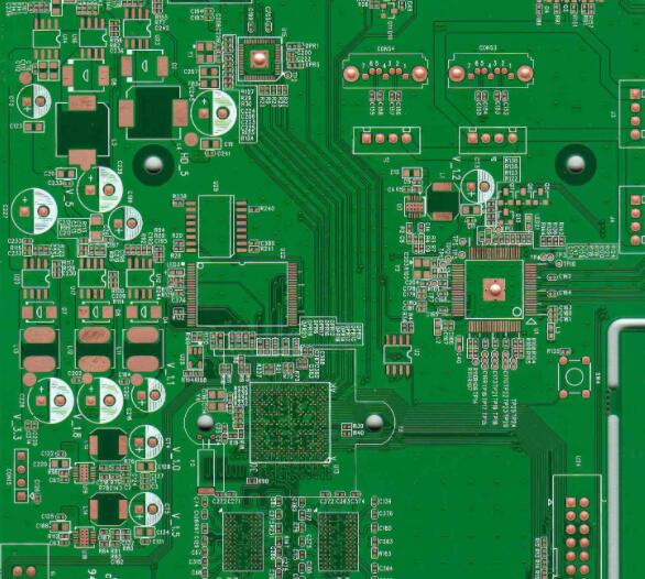
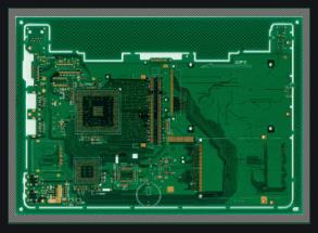
PCB hole plate and solder mask design essentials
1. Orifice plate design in PCB processing
Perforated disk design, including the design of various types of disks with metalized holes and non-metalized holes, these designs are related to the processing capacity of the PCB.
The expansion and contraction of film and material during PCB production, the expansion and contraction of different materials during pressing, the position accuracy of pattern transfer and drilling, etc. will bring about inaccurate alignment between the patterns of each layer. In order to ensure the good interconnection of the patterns of each layer, the width of the pad ring must consider the requirements of the pattern alignment tolerance between the layers, the effective insulation gap and the reliability. Reflected in the design is to control the pad ring width.
(1) The metalized hole pad should be greater than or equal to 5mil.
(2) The width of the insulation ring is generally 10mil.
(3) The width of the anti-pad ring on the outer layer of the metallized hole should be greater than or equal to 6mil, which is mainly proposed in consideration of the needs of solder mask.
(4) The width of the anti-pad ring in the inner layer of the metallized hole should be greater than or equal to 8mil, which mainly considers the requirements of the insulation gap.
(5) The anti-pad ring width of non-metallized holes is generally designed as 12mil.
2. Solder mask design in PCB processing

The minimum solder mask gap, minimum solder mask bridge width, and minimum N cover expansion size depend on the solder mask pattern transfer method, surface treatment process and copper thickness. Therefore, if you need a more precise solder mask design, you need to know about the PCB board factory.
(1) Under the condition of 1OZ copper thickness, the solder mask gap is greater than or equal to 0.08mm (3mil).
(2) Under the condition of 1OZ copper thickness, the width of the solder mask bridge is greater than or equal to 0.10mm (4mil). Since the lm-Sn solution has an attacking effect on some solder resists, the width of the solder mask bridge needs to be increased moderately when using the surface treatment of the lm-Sn, and the minimum is generally 0.125mm (5mil).
(3) Under the condition of 1OZ copper thickness, the minimum expansion size of the conductor Tm cover is greater than or equal to
The solder mask design of the via hole is an important part of the manufacturability design of PCBA processing. Whether to plug holes depends on the process path and the layout of the vias. 9 A& m9 B. Z0 C
(1) There are three main methods for solder mask of via holes: plug hole (including half plug and full plug), open small window and open full window.
(2) Solder mask design of via holes under BGA
For the solder mask of the BGA dog bone connection via hole, we prefer the plug hole design. This has two advantages. One is that it is not easy to bridge due to the offset of the solder mask during BGA reflow soldering; the other is that if the bottom surface of the BGA directly passes the wave crest, it can reduce the soldering and soldering during wave soldering, and the spot is heavy. Melt, affecting reliability.