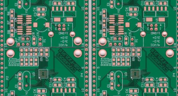
PCB combat skills
When starting a new design, because most of the time is spent on circuit design and component selection, in the PCB layout stage, there is often insufficient experience and insufficient consideration.
If sufficient time and energy are not provided for the design of the PCB layout stage, it may cause problems in the manufacturing stage or defects in the function when the design is transformed from the digital domain to the physical reality.
So what is the key to designing a circuit board that is real and reliable on paper and in physical form? Let's explore the top 6 PCB design guidelines you need to know when designing a manufacturable, reliable PCB.
01. Fine-tune your component layout
The component placement stage of the PCB layout process is both science and art, requiring strategic consideration of the main components available on the circuit board. Although this process can be challenging, the way you place your electronic components will determine how easy your circuit board is to manufacture and how it meets your original design requirements.
Although there is a general order for component placement, such as placing connectors, printed circuit board mounting devices, power circuits, precision circuits, and critical circuits in order, there are some specific guidelines to keep in mind, including:
Orientation-Ensure that similar components are positioned in the same direction, which will help achieve an efficient and error-free welding process.
Arrangement-Avoid placing smaller components behind larger components, so that small components may be affected by the soldering of large components and cause mounting problems.
Organization-It is recommended to place all surface mount (SMT) components on the same side of the circuit board, and place all through-hole (TH) components on the top of the circuit board to minimize assembly steps.

One final PCB design guideline to note-that is, when using mixed technology components (through-hole and surface mount components), the manufacturer may require additional processes to assemble the circuit board, which will increase your overall cost.
Good chip component orientation (left) and bad chip component orientation (right)
Good component placement (left) and poor component placement (right)
02. Properly place power, ground and signal wiring
After placing the components, you can place power, ground, and signal traces to ensure that your signals have a clean and trouble-free path. At this stage of the layout process, keep in mind the following guidelines:
1) Locate the power and ground plane layers
It is always recommended to place the power and ground plane layers inside the circuit board while maintaining symmetry and centering. This helps prevent your circuit board from bending, which is also related to the correct positioning of your components.
For powering the IC, it is recommended to use a common channel for each power supply to ensure a sturdy and stable trace width, and to avoid daisy-chain power connections between components.
2) Signal wire routing connection
Next, connect the signal lines according to the design in the schematic. It is recommended to always take the shortest possible path and direct path between components.
If your components need to be fixed and placed in the horizontal direction without deviation, it is recommended to route the wires basically horizontally where the components of the circuit board go out, and then go through the vertical wiring after the wires are routed.
In this way, with the migration of the solder during soldering, the component will be fixed in the horizontal direction. As shown in the upper part of the figure below. The signal routing method in the lower half of the figure below may cause component deflection as the solder flows during soldering.