Why introduce PCB sample rapid manufacturing system?
At present, electronic technology is developing at an extraordinary speed, and the world electronic product market will surpass the trillion-dollar mark for the first time. In this rapidly developing market, while the performance-price ratio is rising, the product cycle is getting shorter and shorter, averaging only two years. We just know that the products we have just arrived at will be out of date in two or three years. What we use two or three years later is unknown to us today.
This trend is bound to put pressure on electronics designers. A few years ago, it took six to eight months for a product to be conceived and marketed. Now, more complex work needs to be done in a few weeks.
To face the challenge, two innovations must be made: one in the design itself and the other in PCB sample preparation.
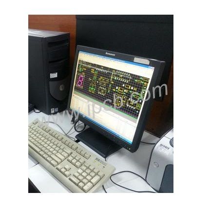
In terms of circuit design, the EDA (Electronic Design Automation-Electronic Design Automation) system has essentially changed the means of electronic product design. Designing with EDA can not only greatly shorten the product development cycle, but also give full play to the experience, wisdom and personality of designers. At present, the function and value of EDA system have been accepted. Computer design system has become the basic configuration of electronic development department. More and more computer systems have jumped onto the platform of electronic designers. More and more Chinese electronic designers, like their counterparts abroad, share the benefits of EDA, a modern tool. EDA technology has made/is making a great contribution to the development of power electronics industry.
However, on the other hand, sample preparation still follows the tradition, offsets the progress of computer design system to some extent, and has become a bottleneck in research and development activities.
In the electronics and microelectronics industry, the design and production of PCB is the most critical link in the product development process. Because most components, devices and integrated circuits can be purchased on the market, only PCBs must be designed and manufactured according to different products. Even products with the same function, even the same circuit, different designers and different companies have different PCBs. It can be said that the characteristics of companies, designers and products are reflected in PCBs. The competition of electronic products is on the one hand the competition of product performance and price, on the other hand the competition of market timing and style characteristics. In essence, these two aspects are closely related to PCB research and development.
In the electronics industry, most engineers are aware of the urgency of the prototype phase. When a new product is about to be put on the exhibition, attend an appraisal meeting, and provide a prototype to users, it is often necessary to design, debug, modify, redesign and debug night and day. At this point, the unit of time is in hours. Sample PCB manufacturing cycles of days or even weeks are simply unacceptable and unacceptable. PCB is called printed PCB because its manufacturing technology invokes printing technology. Similar to printing technology, PCB technology is very suitable for mass production, but very unsuitable for sample PCB production. In ordinary PCB factories, even if it is only a PCB, even if the PCB factories specially provide green channel for the fast board, it also needs data preparation, light drawing version, numerical control data collection and numerical control drilling, hole metallization, film, exposure, development, tin-lead alloy plating, film removal, corrosion and so on. So many processes, so complex technology, naturally require careful production organization, but also naturally need calm time. There is no doubt that such a mechanism is not suitable for providing fast and flexible sample board services.
In today's focus on speed and innovation, in the R&D stage of most products, it is still the order of sample boards to PCB factory. It usually takes a few days to a week, or even a few weeks, from the beginning of contacting the handover design files with PCB manufacturers to getting the PCB. During this time, the electronic designer can only put down the project for the development and design of new projects. After the sample PCB is sent, he can only put down the new project and move on to the previous one. All projects are stuck in the mud, which is not conducive to the designer's inspiration, but also to the project's progress.
Obviously, in terms of speed alone, the traditional sample board mechanism cannot meet the requirements of supply time in the R&D stage, and the market is eager for a new sample board production system.

2. Requirements of Developed Electronic Technology for PCB Sample Board Manufacturing Mechanism
There are three important trends in the development of electronic technology. First, the design and manufacturing cycles have been significantly shortened. Second, continuously miniaturizing; Third, more and more attention has been paid to the environmental impact. Computer design systems and manufacturing technology are the main drivers of such technological progress. The sample PCB production system must adapt to these three trends before it can match the EDA system and become the two wheels driving technological innovation.
First, the sample board making system suitable for the development of contemporary electronic technology should have the ability to make PCB conveniently and quickly. Only in this way can designers grasp every possibility and strive for every advantage. With this system, an electronic designer should design a PCB on an EDA system without the need for cumbersome data handover and transfer. The PCB can be obtained from the CAD data and the component test design results can be installed immediately. Especially when a design needs to be modified repeatedly or there are many ways to achieve it, PCB must be as convenient as drawing and printing. Only in this way can you capture the fleeting inspiration without neglecting the creative passion of the designer. Conversely, if you get a PCB after a week or two or even a month or two, you may even discount the interest of the designer himself, consuming the power of innovation invisibly.
Secondly, the sample board making system must be adapted to the new generation of packaging technology. In order to continuously renovate products and make them outstanding, we need not only a forward-looking awareness, but also the strength to take the lead. Small and delicate are the permanent topics of electronic technology. The electronic products people use, including mobile phones, pagers, laptops and so on, are bound to be lighter, smaller and more powerful. Semiconductor manufacturers started this race early on. SMD components have become the mainstream product in the market, no width of 100 μ And 200 μ The electrical connection between the pins of these elements cannot be achieved by the wires between them. Such fine PCBs must be equipped with advanced equipment and handled carefully before they can be manufactured. Even for first-class professional PCB factories, it is a challenge; For general equipment factories, there will be redundancy and insufficient force, and often the phenomenon of wire edge irregularity, similar disconnection or small insulation gap will affect product performance and research and development quality.
Based on this, the sample PCB production system must have the ability to make PCB with high precision, thin wires and SMD technology. Only in this way can designers be free from the limitations of packaging and sample PCB accuracy, choose the components they want to match EDA technology, and make new generation of packaged, more powerful semiconductor components useful in new products.
Finally, when making sample boards, it should not cause environmental and economic burdens, and let science and technology, people and nature develop in harmony. Such a production system, like an oscilloscope or an EDA system, should become an essential tool in the electronic laboratory, driven by the designer. The general PCB production method is not suitable for the preparation of sample PCB. As we all know, the production of printed PCB has a variety of chemical processes, such as corrosion, pore metallization, electroplating, etc. A large number of chemical materials such as acid, alkali, organic substances are used. Among them are carcinogen formaldehyde, non-degradable substances such as EDTA and organic additives, metal-containing waste liquid and sludge, etc. These substances can cause a great burden on the environment.
At the same time, because of the complex production process, the production mechanism is not suitable for single-piece production, and is not suitable for electronic personnel. Therefore, the sample board making system should adopt a new method different from the traditional process. It is best to achieve what you see is what you get, what you stand for, and to achieve or exceed traditional processes in function and accuracy. On the other hand, it should not pollute the environment and reduce the production costs. It should also be compact and easy to operate.
3. Sample PCB Rapid Manufacturing System Suitable for the Development of Electronic Industry
Since 1976, PCB carving machines have been sold all over the world, and have reached more than 9000. With many years of experience, they have been the exclusive cheese in the latest technology development of PCB carving machine series products. As the industry leader, we have IBM, Motorola, AT&T, Daimler-Chrysler, Nissan, Audi Audi, SEL, Bosch, Siemens Siemens and Hitachi.
The German LPKF rapid PCB production system for electronic laboratories is a set of computer-aided production system, which is combined with the electronic CAD/EDA system to form an independent and complete computer design and verification system.
This system is as compact and simple as a plotter. It connects with a computer designed for PCB through serial port. It can make single panel in more than 10 minutes, double panel in 1-2 hours, and multi-layer board in about 8-12 hours. The design idea is verified immediately. Like computers and EDA software, this device is an indispensable tool in modern electronic design environment.
This system is different from the traditional PCB production process/process, and has no pollution to the environment. It does not need the high investment, large occupancy and serious pollution processes such as light painting, electroless copper plating, film corrosion, etc.
PCB engraver random software reads design data directly, after automatic calculation, the computer drives PCB engraver directly to drill holes on PCB base material. Mill unwanted copper foil along wires and pads with a high-speed rotating mechanical milling cutter to form lines and pads. Mill the small PCB from the base material with an external milling cutter. The system's random CAM software, together with the stencil machine, simplifies the entire PCB production process, eliminating the need for electronics personnel to understand the complex PCB production process and process. The whole process is environmentally friendly and easy to operate.
Operators do not need professional knowledge and experience in PCB production and can operate with simple training.
The use of special cutting tools, combined with the high precision system of the stencil machine, makes it possible to make sample PCBs with line width/spacing of 0.1mm/0.1mm and aperture of 0.3mm in the laboratory. Such thin line widths and spacing, as well as small apertures, make high-density wiring possible, which greatly reduces the size of the PCB.
The rapid panel system can not only make FR-4, FR-3PCB, but also process microwave and radio frequency PCB. The Teflon, RT/duioid microwave panel can be processed with special tools. The side wall of the line is straight and the accuracy is high.
To fit PCB of different densities, LPKF has developed three different ways of pore metallization, which can be summarized as physical pore metallization and chemical pore metallization. Physical pore metallization completely avoids the presence of chemical liquids and is suitable for bottom and medium density PCB.
The advanced direct electroplating process is used for the metallization of chemical holes. The hole conduction can be completed by only four steps of chemical liquid treatment. All chemical solutions contain no harmful HCHO (formaldehyde), lead, EDTA and other substances, all of which are biodegradable. Pharmaceutical liquid is not volatile, can not be discharged or completely sealed during use, so it has no pollution to the environment and meets the requirements of European environmental protection. There is no need to maintain, analyze, or add medicines. It can be used continuously for one year.
Simple, compact presses make it possible to make multilayer plates (up to six layers) in the laboratory. The laminating equipment for making multilayer plates is programmed and easy to operate. For the operator, there is no need for knowledge and experience in multi-layer plate making, just enter the dimensions of the multi-layer plate to be pressed. Low investment and low production cost are another significant feature of LPKF rapid board system.
The SMD installation system is one of the LPKF series devices. With it, you will have a new PCB production plan. The bare panel is finished, the PCB is only half done, and the components need to be installed. SMD mounting system uses surface mounting technology to complete the SMD process and complete the production of sample PCB from the surface. LPKFPCB installation system, including: spot patch film, spot paste, patch, reflux, repairing, testing equipment. Compact design, simple and accurate control, manual operation, bulk and tape components can be mounted, suitable for laboratory and small batch production. It is the solution provided by LPKF fast board system that can not complete sample design, manufacture and component installation at home.
4. Prospects for Rapid Preparation of PCB Samples
The PCB rapid preparation system for LPKF samples has great practicability. Like EDA software, it is a convenient and fast assistant tool for electronic engineers and plays an increasingly important role in the process of electronic design. In the stage of design and development of new products, the efficiency can be greatly improved by using the convenient and fast features of the rapid board system. The system is more flexible during the fault analysis and design phase. Innovation, environmental protection, quality - our philosophy. It is believed that the sample PCB rapid fabrication system of LPKF will be more and more welcomed by Chinese electronic engineers with its convenient, fast, high precision and environmental characteristics, and will also bring benefits to Chinese electronic engineers like EDA software.