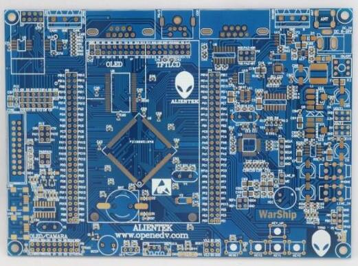
Many friends often hear the word molding in the circuit board industry, but many people can't say what the word specifically means. Let's talk about it in detail below. What are circuit board molding and several methods of shape molding.

Circuit board forming introduction:
Circuit board molding, also called shape, CNC gong board, as the name suggests, is to make the shape that the customer wants according to the shape requirements of the design. The molding is a post-process. After the molding is completed, it is V-CUT, and the board is washed. After testing, packaging, and shipping, the molding method is different according to the order type and the customer's requirements.
Method of circuit board forming:
1, cutting machine:
The cutting machine is an ancient circuit board forming method. Due to the underdeveloped electronic products at that time, many circuit board factories could only use the shearing machine to form the circuit board. The characteristics of the shearing machine are the slow forming speed and the inability to process special-shaped circuit boards.
2, milling machine:
Introduction to circuit board factories Milling machine is the most common forming method among circuit board factories. Its emergence has broken the problem that the shearing machine can not form special shapes because of slow forming. So until now, all the circuit board factories are using milling machines to form circuit boards.
3. Punch:
Punch is a very cumbersome circuit board forming tool, but it is also an indispensable forming tool for every circuit board factory. Some large quantities of circuit boards have more irregular shapes, so the punch is the most suitable forming tool.
4, V slot:
V-slot is to use a V-slot machine to cut the assembled circuit boards. The shape accuracy of the circuit boards processed by the V-slot is relatively low, but the line speed is the fastest among these forming methods.
Discharge tooth
Have you seen other people’s switching power supplies deliberately reserved sawtooth bare copper foil under the common mode inductance? What is the specific effect?
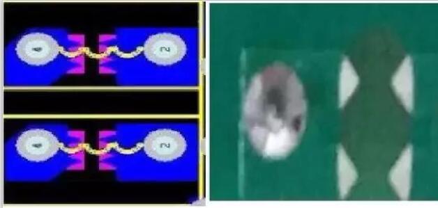
This thing is called discharge tooth, discharge gap or spark gap.

uses spark gap (Sparkgaps) The spark gap is a pair of sharp triangles pointing to each other, the fingertips are separated by a maximum of 10 mils and a minimum of 6 mils. One delta is grounded, and the other is connected to the signal line. This triangle is not a component, but is made by using a copper foil layer in the PCB routing process. These triangles need to be set on the top layer of the PCB (componentside) and cannot be covered by the solder mask.
In the switching power supply surge test or ESD test, high voltage will be generated at both ends of the common mode inductor, and arcing will occur. If it is close to the surrounding devices, the surrounding devices may be damaged. Therefore, a discharge tube or varistor can be connected in parallel to limit its voltage, thereby playing the role of arc extinguishing.
The effect of placing lightning protection devices is very good but the cost is relatively high. Another way is to add discharge teeth at both ends of the common mode inductor during PCB design, so that the inductor discharges through two discharge tips, avoiding discharge through other paths, so as to make the surrounding And the influence of later stage devices is minimized.
The discharge gap does not require additional cost. It is fine to draw it when drawing the PCB board, but it is important to note that this type of discharge gap is an air-type discharge gap, which can only be used in an environment where ESD is occasionally generated.
If used in occasions where ESD occurs frequently, carbon deposits will occur between the two triangular points due to frequent discharges between the discharge gaps, which will eventually cause a short circuit in the discharge gap, and cause permanent short-circuit of the signal line to the ground. Resulting in system failure.