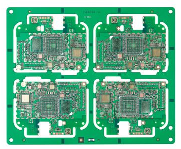
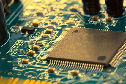
At present, the typical process of printed circuit board (PCB) processing adopts the "pattern plating method". That is, pre-plated a layer of lead-tin anti-corrosion layer on the part of the copper foil that needs to be retained on the outer layer of the board, that is, the pattern part of the circuit, and then chemically corrodes the remaining copper foil, which is called etching. It should be noted that there are two layers of copper on the board at this time. In the outer layer etching process, only one layer of copper must be completely etched away, and the rest will form the final required circuit. This type of pattern electroplating is characterized by the copper plating layer only exists under the lead-tin resist layer. Another process method is to plate copper on the entire board, and the parts other than the photosensitive film are only tin or lead-tin resist. This process is called "full board copper plating process". Compared with pattern electroplating, the biggest disadvantage of copper plating on the whole board is that copper must be plated twice on all parts of the board and all of them must be corroded during etching. Therefore, when the wire width is very fine, a series of problems will occur. At the same time, side corrosion will seriously affect the uniformity of the line.
There is another method in the processing technology of the outer circuit of the printed circuit board, which is to use the photosensitive film instead of the metal plating as the resist layer. This method is very similar to the inner layer etching process, and you can refer to the etching in the inner layer manufacturing process. At present, tin or lead-tin is the most commonly used anti-corrosion layer, used in the etching process of ammonia-based etchant. Ammonia-based etchant is a commonly used chemical liquid, and does not have any chemical reaction with tin or lead-tin. Ammonia etchant mainly refers to ammonia/ammonium chloride etching solution. In addition, ammonia/ammonium sulfate etching chemicals are also available on the market.

Sulphate-based etching solution, after use, the copper in it can be separated by electrolysis, so it can be reused. Because of its low corrosion rate, it is generally rare in actual production, but it is expected to be used in chlorine-free etching. Someone tried to use sulfuric acid-hydrogen peroxide as an etchant to corrode the outer layer pattern. Due to many reasons including economy and waste liquid treatment, this process has not been widely used in a commercial sense. Furthermore, sulfuric acid-hydrogen peroxide cannot be used for the etching of lead-tin resist, and this process is not PCB The main method in outer production, so most people rarely care about it.
2. Etching quality and previous problems
The basic requirement for etching quality is to be able to completely remove all the copper layers except under the resist layer, and that's it. Strictly speaking, if it is to be accurately defined, then the etching quality must include the consistency of the wire width and the degree of undercutting. Due to the inherent characteristics of the current etching solution, which not only produces an etching effect on the downward direction but also on the left and right directions, side etching is almost inevitable.
The problem of side etching is one of the etching parameters that is often raised for discussion. It is defined as the ratio of the width of the side etching to the depth of the etching, which is called the etching factor. In the printed circuit industry, it has a wide range of changes, from 1:1 to 1:5. Obviously, a small undercut degree or a low etching factor is the most satisfactory.
Theoretically, after the printed circuit enters the etching stage, the state of its graphic cross-section. In the process of processing printed circuits by pattern electroplating, the ideal state should be: the total thickness of the electroplated copper and tin or copper and lead tin should not exceed the thickness of the electroplating resistant photosensitive film, so that the electroplated pattern is completely covered on both sides of the film. The "wall" blocks and is embedded in it. However, in actual production, after electroplating circuit boards all over the world, the plating pattern is much thicker than the photosensitive pattern. In the process of electroplating copper and lead-tin, because the plating height exceeds the photosensitive film, a tendency of lateral accumulation occurs, and the problem arises from this. The tin or lead-tin resist layer covering the lines extends to both sides to form a "edge", covering a small part of the photosensitive film under the "edge".
The "edge" formed by tin or lead tin makes it impossible to completely remove the photosensitive film when removing the film, leaving a small part of the "residual glue" under the "edge". The "residual glue" or "residual film" left under the "edge" of the resist will cause incomplete etching. The lines formed "copper roots" on both sides after etching. The copper roots narrowed the line spacing, causing the printed board to not meet the requirements of Party A, and may even be rejected. Rejection will greatly increase the production cost of PCB. In addition, in many cases, due to the formation of dissolution due to the reaction, in the printed circuit industry, the residual film and copper may also form and accumulate in the corrosive liquid and be blocked in the nozzle of the corroding machine and the acid-resistant pump, and it has to be shut down for processing and cleaning., Which affects work efficiency.
3. Equipment adjustment and the interaction relationship with the corrosive solution
In printed circuit processing, ammonia etching is a relatively fine and complex chemical reaction process. On the other hand, it is an easy job. Once the process is up-regulated, production can be continued. The key is to maintain continuous working status once it is turned on, and it is not advisable to dry and stop. The etching process depends to a large extent on the good working condition of the equipment. At present, no matter what etching solution is used, high-pressure spray must be used, and in order to obtain a neater line side and high-quality etching effect, the nozzle structure and spray method must be strictly selected.
In order to obtain a good side effect, many different theories have appeared, forming different design methods and equipment structures. These theories are often very different. But all theories about etching recognize the most basic principle, which is to keep the metal surface in contact with fresh etching solution as quickly as possible. The chemical mechanism analysis of the etching process also confirmed the above point of view. In ammonia etching, assuming that all other parameters remain unchanged, the etching rate is mainly determined by the ammonia (NH3) in the etching solution. Therefore, using fresh solution to etch the surface has two main purposes: one is to flush out the copper ions that have just been produced; the other is to continuously provide ammonia (NH3) needed for the reaction.
4. Regarding the upper and lower board surfaces, the etching state of the leading edge and the trailing edge are different
A lot of problems related to etching quality are concentrated on the etched part of the upper plate surface. It is very important to understand this. These problems come from the influence of the glue-like clumps produced by the etchant on the upper surface of the printed circuit board. The accumulation of colloidal slabstock on the copper surface affects the spraying force on the one hand, and on the other hand prevents the replenishment of fresh etching solution, resulting in a decrease in the etching speed. It is precisely because of the formation and accumulation of colloidal slabs that the degree of etching of the upper and lower patterns of the board is different. This also makes the first part of the board in the etching machine easy to be etched completely or to cause over-corrosion, because the accumulation has not yet formed at that time, and the etching speed is faster. On the contrary, the part that enters behind the board has already formed when it enters, and slows down its etching speed.
5. Maintenance of etching equipment
The most critical factor in the maintenance of etching equipment is to ensure that the nozzle is clean and free of obstructions to make the jet unobstructed. Blockages or slagging will impact the layout under the action of jet pressure. If the nozzle is not clean, it will cause uneven etching and scrap the entire PCB. Obviously, equipment maintenance is the replacement of damaged and worn parts, including replacement of nozzles. The nozzles also have the problem of wear. In addition, the more critical issue is to keep the etching machine free of slagging. In many cases, slagging will accumulate. Excessive slagging will even affect the chemical balance of the etching solution. Similarly, if there is excessive chemical imbalance in the etching solution, slagging will become more serious. The problem of slag accumulation cannot be overemphasized. Once a large amount of slagging occurs suddenly in the etching solution, it is usually a signal that there is a problem with the balance of the solution. This should be done with strong hydrochloric acid for proper cleaning or supplementation of the solution.