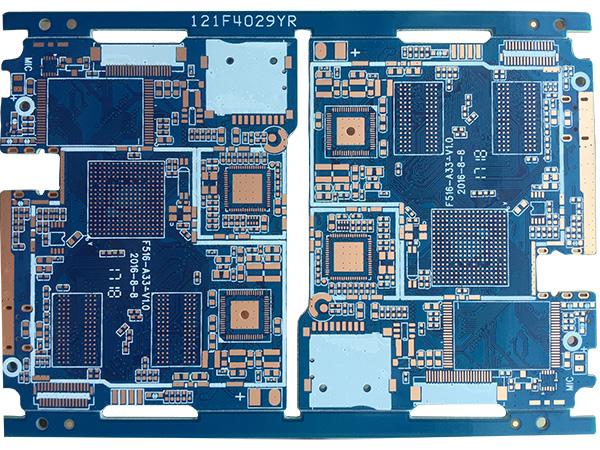
According to the printed circuit board wiring, let's take a look below.
1. Wire
(1) Width
The extremely small width of the printed wire is mainly determined by the adhesion strength between the wire and the insulating substrate and the current value flowing through them. The printed wire can be as wide as possible, especially the power line and ground wire, as wide as possible under the condition of the board surface, even if the area is tight, it is generally not less than 1mm. Especially the ground wire, even if it is not allowed to be widened locally, it should be widened where it is allowed to reduce the resistance of the entire ground wire system. For wires whose length exceeds 80mm, even if the operating current is not large, they should be widened to reduce the influence of the voltage drop of the wires on the circuit.
(2) Length
To minimize the length of the wiring, the shorter the wiring, the less interference and crosstalk, and the lower the parasitic reactance and the less radiation. Especially the grid of the field effect tube, the base of the triode and the high-frequency circuit should pay attention to the wiring to be short.

(3) interval
The spacing between adjacent wires should meet the requirements of electrical safety. Crosstalk and voltage breakdown are the main electrical characteristics that affect the wiring spacing. In order to facilitate operation and production, the interval should be as wide as possible, and the smallest interval selected should at least be suitable for the applied voltage. This voltage includes operating voltage, additional shaking voltage, overvoltage and peak voltage due to other reasons. When there is mains voltage in the circuit, the interval should be wider for safety.
(4) Route
The width of the signal path should be constant from drive to load. Changing the path width will change the path impedance (resistance, inductance, and capacitance), and reflection and imbalance of line impedance will occur. Therefore, the width of the path remains unchanged. In wiring, avoid using right angles and sharp angles. Generally, the corner should be greater than 90°. A concentrated electric field can occur at the inner margin of the right-angle path, and the electric field generates noise coupled to the adjacent path. The 45° path is better than the right-angle and acute-angle paths. When two wires meet and join at an acute angle, the acute angle should be changed to a circle.
2, aperture and pad size
According to the diameter of the component device hole in the PCB circuit board, the diameter of the component lead should be better matched, so that the diameter of the device hole is slightly larger than the component lead diameter (0.15 ~ 0.3) mm. Generally, DIL package pins and most small components use 0.8mm aperture, and the diameter of the pad is about 2mm. For large-aperture pads, in order to obtain better adhesion, the ratio of the diameter of the pad to the aperture is about 2 for the epoxy glass base, and (2.5~3) for the phenol cardboard base.
Vias are generally used in multi-layer .PCB designs Its smaller usable diameter is related to the thickness of the board base. Generally, the ratio of the board base thickness to the via diameter is 6:1. In the case of high-speed signals, via holes generate (1~4) nH inductance and (0.3~0.8) pF capacitance. Therefore, when laying high-speed signal channels, the vias should be kept extremely small. Regarding high-speed parallel lines (such as address and data lines), if layer changes are inevitable, you should ensure that the number of vias for each signal line is the same. And the number of vias should be reduced as much as possible. If necessary, a printed wire maintenance ring or maintenance line should be set to avoid oscillation and improve circuit functions.