Now, communication products, computers and almost all other electronic products use printed circuits. The development and improvement of printed circuit technology created conditions for the advent of integrated circuits, an invention that changed the face of the world. With the development of science and technology, printed circuit boards are widely used in high-tech fields such as military industry, communications, medical treatment, electric power, automobiles, industrial control, smart phones, and wearables.
The invention of the printed circuit
The printed circuit was invented by Austrian electrical engineer Paul Eisler in the mid-1930s. Eisler studied electrical engineering at the Vienna School of Engineering in his early years. After graduating in 1930, he studied printing technology. When he was researching electronic circuit boards, he often went to the library to check books and periodicals on printing technology.
After serious thinking, he came up with an idea: If you print the circuits of electronic devices on the circuit boards at a time, like printing books or newspapers, you don’t need to make the circuit boards piece by piece by hand, and there is no need for people to make the circuit boards one by one. After the ground is welded, the production efficiency and reliability of electronic products can be greatly improved.
When Eisler manufactures circuit boards, it also uses a plate-making method similar to that of the printing industry. He first drew the electronic circuit diagram, and then etched the circuit diagram on the insulating board covered with a layer of copper foil, so that the unnecessary copper foil was etched away, leaving only the conductive circuit. In this way, the various electronic components are connected to each other through the circuit formed by the copper foil on this board. This kind of printed circuit can not only improve the reliability of electronic products, but also greatly improve production efficiency, which has great value and potential for the development of new electronic products.

The use of printed circuit technology makes the mass production of electronic equipment simple and easy, laying the foundation for the mechanized and automated production of electronic products. Since the 1950s, the substantial progress made in various electronic products, including communication equipment, is inseparable from the use of printed circuit technology.
With the continuous improvement of the manufacturing level of printed circuits, the printed circuits produced can reach high precision, thus pushing the production and manufacturing of circuit boards to a new stage. When making plates in the printing industry, a large picture can be reduced to a certain size by shooting.
When manufacturing printed circuits, the electronic circuit diagram can also be reduced to make a plate, making it an electronic circuit board with a small area, complex circuits and high reliability. This kind of printed circuit board is very suitable for communication equipment and computers with complex circuits and high reliability requirements. The development of printed circuit technology laid the necessary technical foundation for the subsequent invention of integrated circuits.
The circuit board has a history of more than 60 years since its invention. History has shown that: without circuit boards, without electronic circuits, flying, transportation, atomic energy, computers, aerospace, communications, home appliances... all of this cannot be achieved.
The reason is easy to understand. Chips, ICs, and integrated circuits are the food of the electronic information industry. Semiconductor technology reflects a country's industrial modernization level and guides the development of the electronic information industry. The electrical interconnection and assembly of semiconductors (integrated circuits, ICs) must rely on circuit boards.
Types of printed circuit boards
The printed circuit boards used in actual electronic products are very different, and there are different classifications according to different standard printed circuit boards.
Classified by the distribution of printed circuits
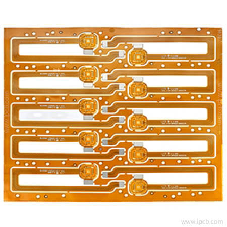
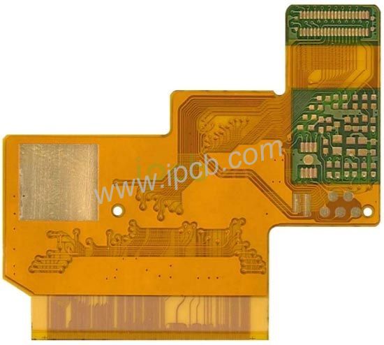
According to the approximate distribution of the printed circuit, the printed circuit board can be divided into three types: single panel, double panel, and multi-layer board.
The single-sided board is at a thickness of o. On the insulating substrate of 2-5mm, only one surface is covered with copper foil, and a printed circuit is formed on the substrate by printing and etching. The single panel is simple to manufacture and easy to assemble. It is suitable for the requirements of a circuit, such as radios, televisions, etc.; it is not suitable for occasions that require high assembly density or complex circuits.
Double panel
Printed circuit boards in the field of electronic components
The double-sided board is at a thickness of o. Circuits are printed on both sides of the 2-5mm insulating substrate. It is suitable for electronic products with general requirements, such as electronic computers, electronic instruments and meters. Since the wiring density of the double-sided printed circuit is higher than that of the single-sided printed circuit, the volume of the device can be reduced.
Multilayer board
Printed boards with more than 3 layers of printed circuits printed on an insulating substrate are called multilayer boards. It is made up of several thin single-sided or double-sided boards, and its thickness is generally 1.2-2.5m. In order to lead out the circuit sandwiched between the insulating substrate, the holes for mounting components on the multilayer board need to be metalized, that is, a metal layer is applied to the inner surface of the small holes to connect them with the printed circuit sandwiched between the insulating substrates.