Although printed circuit board (PCB) and printed circuit board assembly (PCBA) are often used interchangeably, they are not the same. So what is the difference between PCB and PCBA?
You can define a PCB as a board on which electronic components can be mounted to complete the planned circuit. On the contrary, PCBA refers to a board on which all components and parts have been soldered and mounted on the PCB and are ready to perform its programmed electronic functions.
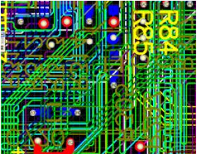
Today, PCBs are small, multi-layered, and complex, and hardly your earliest ancestors. Thanks to advanced design tools and production methods, the production speed of this product is much higher than before, and it is more efficient. Even ten years ago, only the most expensive prototypes for HDI and FPGA were seen, but these designs are now available worldwide.
Basic components of a printed circuit board (PCB)
The PCB is made of a conductive trace design and a substrate usually made of glass epoxy material. For example, a simple PCB can be divided into four, six or eight layers, while the more common four and six layers can be. PCB design is printed parts or printed circuits, or a combination of both. The conductive design is printed or engraved on insulating epoxy glass that can be given a preset pattern.

PCB is designed for electronic products, such as TVs, mobile phones and PC components. They are also used to manufacture lighting and medical equipment, industrial machinery. PCB is an important part of the system structure because it helps electronic equipment and serves as the electrical connection of components. The unique features of PCB are:
Thin and light Suitable for connecting multiple electronic components in a compact space.
Due to its graphic accuracy and repeatability, the equipment can be maintained, debugged and inspected.
Production can be automated to minimize the cost of electronic equipment.
PCB type
There are several types of PCBs. In particular, PCB has four main forms, they are:
Single-sided PCB
A single-layer or single-sided PCB is a single layer composed of a substrate or a substrate. One side of the base material is coated with a thin layer of metal. Copper is the most widely used coating because it can be used well as an electrical conductor.
Double-sided PCB
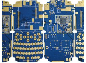
Both sides of the substrate of a double-sided or double-sided PCB are equipped with a base material including copper and a conductive metal film. Holes through the board allow circuits on one side of the board to connect to circuits on the other side. Circuits and components on a double-layer PCB are usually connected in one or two ways; through through or using surface mount.
Multilayer PCB
A series of three or more double-layer PCBs consists of multilayer PCBs. These boards are then laminated with cores between advanced prepregs and insulating components to prevent excessive heat from melting any components. The size of multi-layer PCBs varies from 4 to 10 or 12 layers. On a commercial scale, the maximum number of layers created in the multi-storey built in history is 50.
Flexible PCB
Compared with rigid PCBs that use non-movable materials (such as fiberglass), flexible PCBs are made of materials that can move and bend like plastic. Flexible PCBs can be in single-layer, double-layer or multi-layer formats, just like rigid PCBs. Their production costs are often higher because they must be printed on flexible materials.
Rigid and flexible PCB
A rigid flexible PCB is a combination of a rigid circuit board and a flexible circuit board. They consist of multiple layers of flexible circuits attached to more than one rigid board.
These PCBs are precision manufactured. Therefore, it is used in various military and medical applications.
These PCBs are light in weight, which can reduce weight by 60% and save space.
High frequency PCB
The high frequency PCB is used in the frequency range of 500MHz to 2GHz. These PCBs are used in various frequency-critical applications, such as communication systems, microwave PCBs, and microstrip PCBs.
How is the PCB designed?
The first step is to use software (such as Altium) to print the circuit design, and then use a plotter printer to print. The inner layer is represented by two colors of ink: black represents the copper wire, and white represents the non-conductive area of the PCB. This process is reversed on the outer layer.
The second step is to print copper on the inner layer, then remove the unwanted copper, then check the alignment of the layers, and use the layer sensor for optical inspection.
The third step after inspection involves laminating the PCB layers and then drilling holes in the panel. After the panel drilling process, the PCB board process starts with the use of chemicals to melt all the different PCB layers. Then, imaging and silver plating of the outer layer takes place, which involves an etching process to obtain the best results.
Why does it make the PCB strong enough to hold the assembled components?
The substrate used for PCB processing and printing is usually glass fiber reinforced epoxy resin. The manufacture of high-end boards is to reinforce glass fiber and epoxy resin with copper foil. Connect to one or both sides of the substrate. A board made of phenolic resin and reinforced with paper and molten copper foil; it seems to be cheaper.
The key point to remember when choosing a PCB/PCBA is that a PCB is just a circuit board with printed circuits. PCBA is a complete software package; it has all the necessary and available components for your desired purpose.
Why is PCB assembly essential in product development?
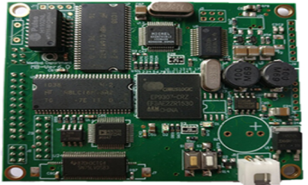
As mentioned earlier, a PCB with additional components is called an assembled PCB, and the manufacturing process is simply called PCB Assembly or PCBA. These tiny green chips are encapsulated in copper wires located in components in the center of the destroyed electronic components. Their frame is made of fiberglass, copper and other metal components and is worn with epoxy resin and insulated by solder mask.
On a single board, copper wires called traces electrically connect connectors and components. These functions operate signals to allow the circuit board to operate in a specific way. These functions range from basic to complex, but the size of the PCB can still be smaller than the size of the thumbnail.
PCBA components
Refill or repackage electronic components with empty PCB boards to create an effective printed circuit board (PCA) or PCBA during the assembly process. With hole technology, electronic components are placed in holes surrounded by conductive pads. SMT places the pins on the PCB to ensure that the pins match the conductive pads.
Before soldering, the electronic component fixing parts on both sides of the circuit board must be glued to one side of the circuit board. The standard procedure for testing PCB components is as follows.
With the power turned off or using an automatic optical inspection tool, visually inspect the circuit board.
Shutdown is used to perform analog signature analysis. This investigation is called a "shutdown check".
The online test is carried out through the power supply.
Finally, a bump test is performed to determine whether the PCB is performing its work.
PCB VS PCBA: Reliability Analysis
Manufacturing process
Since the PCB does not require assembly, it is easier to manufacture. In view of the complexity of PCBA, because different modules must be connected, and with it is the oven soldering at the connection.
cost
The cost of producing a PCB for the same board is much lower than the cost of manufacturing a PCBA system. Additional PCBA projects also have considerable costs, which adds to the total cost of completed PCBA.
Feature
The PCB is an empty board. It has no components for transmitting power. On the contrary, PCBA is equipped with all the necessary components and can be used.
Package
PCB adopts vacuum packaging, while PCBA board adopts isolation or antistatic packaging.
Key points: Without PCBA, PCB cannot work normally
The function of the PCB can only be realized after assembly. Therefore, the terms PCB and PCBA are widely related. Some key points of this article are as follows.
Conceptual difference: PCB stands for bare circuit board, while PCBA stands for PCB board equipped with components using plug-in assembly or SMT assembly process. PCBA should be understood as a complete circuit board, but the PCBA cannot be calculated until the circuit board is equipped with the components required for its function. These components are usually electronic chips, cables and other electronic parts. However, because PCBs have various packages and specifications, there are more. Common PCBs are made of epoxy glass resin and are divided into 4-layer, 6-layer and 8-layer boards; it depends on the number of signal layers.
PCB is undoubtedly the basic component of all electrical systems. Our society relies on the successful implementation of circuit boards to handle affairs effectively. If this basic technology fails, all human electrical systems will be unusable.
Generally speaking, both PCB and PCBA have potential potential. We are always moving towards better designs and the ability to adapt to ultra-complex functions on small circuit boards.