I believe that many people are not unfamiliar with PCB circuit boards, and may be heard often in daily life, but they may not know much about PCBA, and may even be confused with PCB. So what is a PCB? How did PCBA evolve? What is the difference between PCB and PCBA? Let's take a look at it in detail below.
*About PCB*
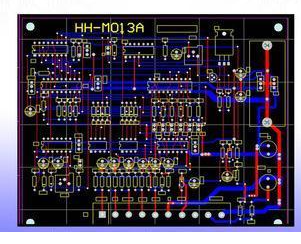
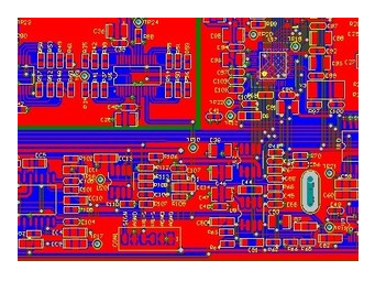
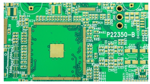
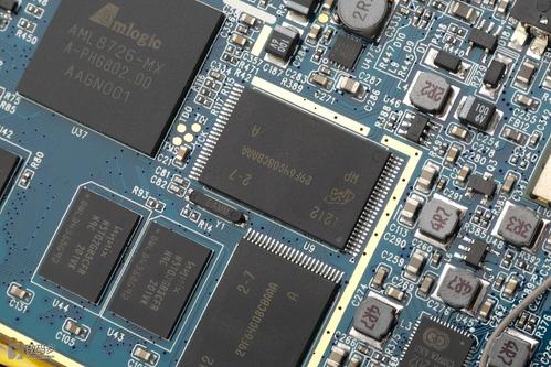
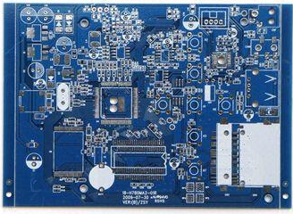
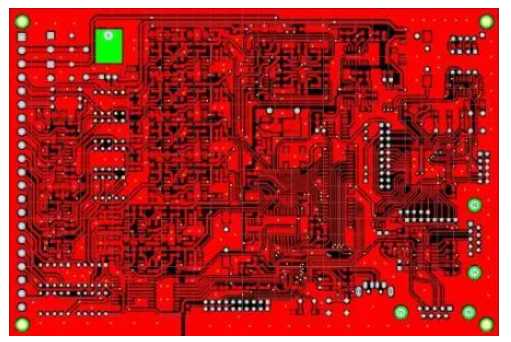
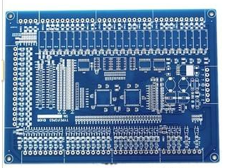
PCB is the abbreviation of Printed Circuit Board, translated into Chinese is called printed circuit board, because it is made by electronic printing, it is called "printed" circuit board. PCB is an important electronic component in the electronics industry, a support for electronic components, and a carrier for electrical connection of electronic components. PCB has been extremely widely used in the manufacture of electronic products. The unique characteristics of PCB are summarized as follows:
1. High wiring density, small size and light weight, which is conducive to the miniaturization of electronic equipment.
2. Due to the repeatability and consistency of the graphics, the wiring and assembly errors are reduced, and the maintenance, debugging and inspection time of the equipment is saved.
3. It is conducive to mechanization and automatic production, which improves labor productivity and reduces the cost of electronic equipment.
4. The design can be standardized to facilitate interchangeability.
*About PCBA*
PCBA is the abbreviation of Printed Circuit Board + Assembly, which means that PCBA passes through the entire manufacturing process of PCB blank board SMT and then DIP plug-in.
Note: SMT and DIP are both ways to integrate parts on the PCB. The main difference is that SMT does not need to drill holes on the PCB. In DIP, the PIN pins of the parts need to be inserted into the holes that have been drilled.
SMT (Surface Mounted Technology) surface mount technology mainly uses mounters to mount some tiny parts on the PCB. The production process is: PCB board positioning, solder paste printing, mounter mounting, and reflow Furnace and finished inspection.
DIP stands for "plug-in", that is, inserting parts on the PCB board. This is the integration of parts in the form of plug-ins when some parts are larger in size and are not suitable for placement technology. The main production process is: sticking adhesive, plug-in, inspection, wave soldering, printing and finished inspection.
*The difference between PCB and PCBA*

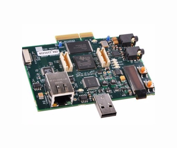
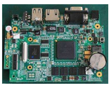
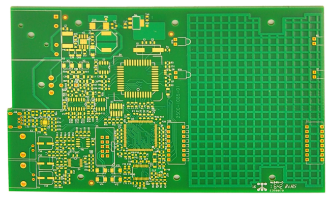
From the above introduction, we can know that PCBA generally refers to a processing process, which can also be understood as a finished circuit board, that is, PCBA can be counted after all the processes on the PCB board are completed. The PCB refers to an empty printed circuit board with no parts on it.
In general: PCBA is a finished board; PCB is a bare board.
COB requirements for PCB design
Since COB does not have a lead frame for IC packaging, it is replaced by PCB. Therefore, the design of the PCB pad is very important, and Finish can only use electroplated gold or ENIG, otherwise gold wire or aluminum wire, or even The latest copper wire will have the problem of not being able to reach it.
1. The surface treatment of the finished PCB board must be electroplated gold or ENIG, and it must be a little thicker than the general PCB gold plating layer to provide the energy required for Die Bonding to form a gold-aluminum or gold-gold co-gold.
2. In the wiring position of the solder pads outside the COB Die Pad, try to make sure that the length of each solder wire has a fixed length, which means that the distance between the solder joints from the wafer to the PCB solder pads should be as consistent as possible, so The position of each welding wire can be controlled, and the problem of short-circuiting of the welding wires can be reduced. Therefore, the diagonal pad design does not meet the requirements. It is suggested that the PCB pad spacing can be shortened to eliminate the appearance of diagonal pads. It is also possible to design elliptical pad positions to evenly disperse the relative positions between the welding wires.
3. It is recommended that a COB wafer should have at least two positioning points. It is best not to use traditional SMT circular positioning points for positioning points, but use cross-shaped positioning points, because the Wire Bonding machine is doing automatic Basically, the positioning will be done by grasping a straight line. I think this is because there is no circular positioning point on the traditional lead frame, but only a straight outer frame. Some Wire Bonding machines may be different. It is recommended to design with reference to the performance of the machine first
4. The Die Pad size of the PCB should be slightly larger than the actual wafer. One can limit the deviation when placing the wafer, and it can also prevent the wafer from rotating too severely in the die pad. It is recommended that the wafer pads on each side are 0.25~0.3mm larger than the actual wafer.
PCB design
5. It is best not to have via holes in the area where COB needs to be filled with glue. If it cannot be avoided, then the PCB factory is required to completely plug these via holes 100%, in order to avoid the penetration of the via holes into the PCB during Epoxy dispensing. On the other side, causing unnecessary problems.