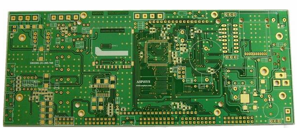
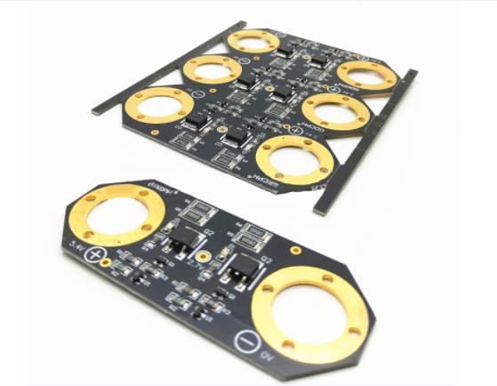
SMD LED is a new type of surface-mounted semiconductor light-emitting device, which has the advantages of small size, large scattering angle, good luminous uniformity, and high reliability. The luminous color includes various colors including white light, so it is widely used in Various electronic products. PCB board is one of the main materials for manufacturing SMD LEDs. The development of each new SMD LED product starts from the design of the PCB board drawing. The front and back graphics of the PCB, the SMD LED assembly drawing and the finished product drawing should be given during the design, and then the designed PCB board drawing It is designed for professional LED PCB board manufacturers. The quality of the design directly affects the quality of the product and the implementation of the manufacturing process.
Designing a perfect SMD LED PCB board is not an easy task, and many factors affecting the design must be considered. To this end, the PCB copy board technicians of Dongdao Technology will discuss the design of the SMD LED PCB board from the following aspects through practice and multi-party data sorting.
1. SMD LED PCB board structure selection
The types of SMD LED PCB boards are classified according to the structure: through-hole structure, slot-digging structure, etc.; according to the number of chips used in a single SMD LED: single crystal, double crystal and triple crystal. The difference between the through-hole structure PCB board and the slotted-hole structure PCB board is that the former needs to be cut in two directions when cutting, and a single finished electrode is half-arc; the latter only needs to be cut in one direction when cutting. The choice of what kind of structure PCB board and SMD LED adopt several chips is based on the requirements of market users. When the user does not put forward special requirements, the PCB board is usually designed with a slotted hole structure. The PCB substrate is a BT board.

Second, the choice of slotting direction
If you choose to design the PCB board with a slotted hole structure, you must consider which direction to choose for the slotted hole. Under normal circumstances, the slotted hole is designed along the width of the PCB board, because this can minimize the deformation of the PCB board after the compression molding.
Three, PCB board outline size selection
The factors that must be considered in the selection of the size of each new SMD LED PCB board: 1. The number of products designed on each PCB board is required. 2. Whether the deformation degree of the PCB board is within the acceptable range after compression molding.
Without affecting the production process, the number of products on each PCB board should be designed as many points as possible, which will help reduce the cost of a single product. In addition, since the colloid will shrink after compression molding, the PCB board is prone to deformation, so when designing the PCB board, the number of SMD LEDs in each group should not be too much, but the number of groups can be designed more. In this way, the requirement of the number of SMD LEDs on a single PCB board can be met, and the PCB board deformation caused by the shrinkage of the colloid after the compression molding will not be too large. The large deformation of the PCB board will cause the PCB board to be unable to be cut and the glue and the PCB board will easily peel off after cutting.
The thickness of the PCB board is selected according to the overall thickness requirements of the SMD LED used by the user. The thickness of the PCB board should not be too thick, too thick will cause the wire bonding after die bonding; the thickness of the PCB board should not be too thin, too thin will cause the PCB board to deform too much due to the shrinkage of the colloid after the compression molding is formed.
Take the ordinary SMD LED product with the thickness of 0603 specification of 0.6mm as an example. If a PCB board with a thickness of 0.3mm is selected, the thickness of the colloid part can only be 0.3mm, and then a wafer with a thickness of 0.28mm is selected for die bonding. The overall thickness is already 0.58mm, and the wire bonding operation cannot be performed. If the thickness of the PCB board is 0.1mm, the thickness of the colloid part is 0.5mm, and the colloid shrinks significantly after the compression molding is formed because the colloid is thicker, and the PCB board is thin, which will cause excessive deformation of the PCB board. Therefore, when designing the thickness of the PCB board, an appropriate thickness must be selected, which can make the same PCB board suitable for chip-on-chip LEDs of different thicknesses, without causing excessive deformation of the PCB board after compression molding.
Four, PCB board circuit design requirements
1. Die-bonding zone: The size design of the die-bonding zone is determined by the size of the wafer. Under the condition that the chip can be securely fixed, the die-bonding area should be designed as small as possible. In this way, the adhesion between the glue and the PCB board will be better after the compression molding, and it is not easy to cause the phenomenon of peeling of the glue and the PCB board. At the same time, it is also necessary to consider the design of the die bonding area as much as possible in the middle of the single SMD LED circuit board.
2. Wire bonding area: The wire bonding area is basically larger than the size of the bottom of the magnetic nozzle.
3. The distance between the die bond area and the wire bond area: The distance between the die bond area and the wire bond area should be determined by the wire arc of the wire. Large distance will cause insufficient wire arc tension, and small distance will cause the gold wire to touch the chip during wire bonding.
4. Electrode width: The electrode width is generally 0.2mm.
5. Circuit wire diameter: The size of the circuit wire connecting the electrode and the die bonding area should also be considered. Using a small wire diameter can increase the adhesion between the substrate and the colloid.
6. Via hole diameter: If the PCB board is designed with via holes, the minimum via hole diameter is generally Φ0.2mm.
7. Slotted hole aperture: If a through hole is used to design the PCB board, the minimum width of the slotted hole is generally 1.0mm.
8. Cutting line width: due to the existence of a certain thickness of the cutting blade during cutting, a part of the PCB board will be worn after cutting. Therefore, the thickness of the cutting blade should be considered when designing the cutting line width, and compensation should be made in the design of the PCB board. Otherwise, the width of the finished product will be narrow after cutting.
In addition, the aperture size of the positioning hole must also be considered. Generally, the number of products within the designable circuit range of a PCB board is designed to be an even number.
Five, the quality requirements for PCB substrates
When designing the PCB board, the following technical descriptions should be made for the production of the PCB board:
1. Sufficient accuracy is required: the unevenness of the board thickness is required to be <±0.03mm, and the deviation of the positioning hole to the circuit board circuit is <±0.05mm.
2. The thickness and quality of the gold-plated layer must ensure that the tensile test of the gold wire after bonding> 8g.
3. After the PCB board is made into a finished product, it is required that the surface is free of dirt, and the adhesion between the mold and the glue is good.