The reliability of electronic equipment will decline, and even electronic equipment will fail due to overheating of the device. Therefore, it is very important to conduct heat dissipation design processing on the circuit board.
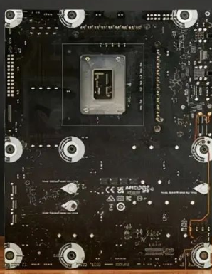
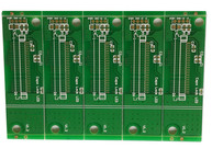
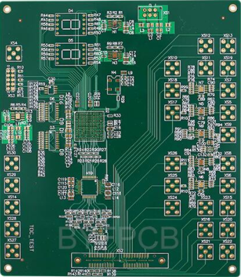
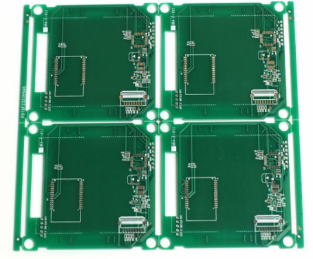
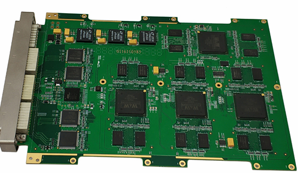
The printed circuit board, that is, the PCB board, is based on the schematic diagram of the circuit and realizes the functions required by the circuit designer. PCB board design includes layout design, which needs to consider various factors such as the layout of external connections, the optimized layout of internal electronic components, the optimized layout of metal connections and through holes, electromagnetic protection, and heat dissipation.
PCB temperature rise factor analysis
The direct cause of the temperature rise of the printed board is due to the existence of circuit power consumption devices. Electronic devices all have power consumption to varying degrees, and the heating intensity varies with the size of the power consumption.
Two phenomena of temperature rise in printed boards:
(1) Local temperature rise or large area temperature rise
(2) Short-term temperature rise or long-term temperature rise

Ways to improve the temperature rise of PCB printed boards need to be considered in many aspects, because these factors are often interrelated and dependent in a product and system, most of the factors should be analyzed according to the actual situation, only for a specific The actual situation can calculate or estimate the parameters such as temperature rise and power consumption more correctly.
Circuit board heat dissipation method
Therefore, when analyzing and designing PCB thermal power consumption, the following aspects are generally used to solve the PCB heat dissipation method and optimize the design.
1. High heat-generating device plus radiator, heat conduction plate (tube)
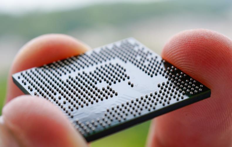
When a small number of components in the PCB generate a large amount of heat (less than 3), a heat sink or heat pipe can be added to the heating device. When the temperature cannot be lowered, a heat sink with a fan can be used to enhance heat dissipation Effect. When the number of heating devices is large (more than 3), a large heat sink (tube) can be used, which is a special radiator customized according to the position and height of the heating device on the PCB or a large flat radiator Cut out different component height positions. The heat dissipation cover is integrally buckled on the surface of the component, and it is in contact with each component to dissipate heat. However, the heat dissipation effect is not good due to the poor consistency of height during assembly and welding of components. In recent years, soft thermal phase change thermal pads will be added to the surface of some high-heat components to improve the heat dissipation effect.
2. Heat dissipation through the PCB board itself
At present, the widely used PCB boards are copper-clad/epoxy glass cloth substrates or phenolic resin glass cloth substrates, and a small amount of paper-based copper-clad boards are used.
Although these substrates have excellent electrical properties and processing properties, they have poor heat dissipation. As a heat dissipation path for high-heating components, it is almost impossible to expect heat from the resin of the PCB itself to conduct heat, but to dissipate heat from the surface of the component to the surrounding air. However, as electronic products have entered the era of miniaturization of components, high-density mounting, and high-heating assembly,
It is not enough to rely on the surface of a component with a very small surface area to dissipate heat. At the same time, due to the extensive use of surface mount components such as QFP and BGA, a large amount of heat generated by the components is transferred to the PCB board. Therefore, the best way to solve the problem of heat dissipation is to improve the heat dissipation capacity of the PCB itself, which is in direct contact with the heating element, through the PCB board. To be transmitted or emitted.
3. Use reasonable wiring design to achieve heat dissipation
Because the resin in the plate has poor thermal conductivity, and the copper foil lines and holes are good conductors of heat, increasing the residual rate of the copper foil and increasing the thermally conductive holes are the main means of heat dissipation. To test and evaluate the heat dissipation capacity of a PCB, it is necessary to calculate the equivalent thermal conductivity of a composite material composed of various materials with different thermal conductivity-an insulating substrate for PCB.
4. Reasonable and even distribution of heat sources
The components on the same printed board should be arranged as far as possible according to their calorific value and degree of heat dissipation. Devices with low calorific value or poor heat resistance (such as small signal transistors, small-scale integrated circuits, electrolytic capacitors, etc.) should be placed in the cooling airflow. The uppermost flow (at the entrance), the devices with large heat or heat resistance (such as power transistors, large-scale integrated circuits, etc.) are placed at the most downstream of the cooling airflow. Avoid the concentration of hot spots on the PCB, distribute components with equivalent power evenly on the PCB board as much as possible, and keep the PCB surface temperature performance uniform and consistent.
5. Use thermal conductive materials to reduce thermal resistance
High heat dissipation devices should minimize the thermal resistance between them when they are connected to the substrate. In order to better meet the thermal characteristics requirements, some thermal conductive materials (such as a layer of thermally conductive silica gel) can be used on the bottom surface of the chip, and a certain contact area can be maintained for the device to dissipate heat.
6. The connection between the device and the substrate
(1) Minimize the lead length of the device
(2) When selecting high-power devices, the thermal conductivity of the lead material should be considered. If possible, try to choose the largest cross section of the lead
(3) Choose a device with more pins
7. Selection of packaging materials for devices
(1) When considering PCB therma l design, pay attention to the package description of the device and its thermal conductivity
(2) Consider providing a good heat conduction path between the substrate and the device package
(3) Air partitions should be avoided in the heat conduction path. If this is the case, heat-conducting materials can be used for filling.