For electronic products, PCB board design is a design process necessary for it to change from an electrical schematic diagram to a specific product. The rationality of its design is closely related to product production and product quality. For many people who are just engaged in electronic design In other words, there is less experience in this area. Although PCB design software has been learned, the PCB boards designed often have such problems.
The usual order of placing the components on the PCB board:
1. Place the components in a fixed position that closely match the structure, such as power sockets, indicator lights, switches, connectors, etc. After these components are placed, use the LOCK function of the software to lock them, so that they will not be mistaken in the future move;
2. Place special components and large components on the circuit, such as heating components, transformers, ICs, etc.;
3. Place small devices.
The distance between the components and the edge of the PCB board:

If possible, all components should be placed within 3mm from the edge of the PCB or at least greater than the thickness of the PCB. This is because in mass production of assembly line plug-ins and wave soldering, they must be provided to the guide groove for use, and also to prevent Due to the defect of the edge part caused by the shape processing, if there are too many components on the PCB board, if it is necessary to exceed the range of 3mm, you can add a 3mm auxiliary edge to the edge of the PCB board, and open the V-shaped groove on the auxiliary edge. Just break it.
Isolation between high and low pressure:
There are high-voltage circuits and low-voltage circuits on many PCB boards at the same time. The components of the high-voltage circuit parts and the low-voltage parts should be placed separately. The isolation distance is related to the withstand voltage to be withstand. Normally, the distance between the PCB board and the PCB board is 2mm at 2000kV., If you want to withstand the 3000V withstand voltage test, the distance between the high and low voltage lines should be more than 3.5mm. In many cases, it is still on the PCB to avoid creeping. Slotting between the high and low pressure.
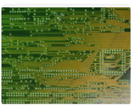
PCB board routing:
The layout of printed wires should be as short as possible, especially in high-frequency circuits; the bends of printed wires should be rounded, and right or sharp corners will affect electrical performance in high-frequency circuits and high wiring density. ; When the two panels are wired, the wires on both sides should be perpendicular, oblique, or bent to avoid parallel to each other to reduce parasitic coupling; printed wires used as the input and output of the circuit should be avoided as far as possible. In order to avoid feedback, it is best to add a ground wire between these wires.
Width of printed wire:
The width of the wire should be able to meet the electrical performance requirements and facilitate PCB production. Its minimum value is determined by the magnitude of the current it can withstand, but the minimum should not be less than 0.2mm. In high-density, high-precision printed circuits, the wire width and spacing are generally 0.3mm; the wire width should also consider its temperature rise in the case of large currents. The single-panel experiment shows that when the thickness of the copper foil is 50μm and the wire width is 1 The temperature rise is very small when the current is ~1.5mm and the current is 2A. Therefore, it is possible to meet the design requirements without causing a temperature rise by using a wire with a width of 1 ~ 1.5mm.
The common ground wire of the printed wire should be as thick as possible. If possible, use a line larger than 2 to 3 mm. This is particularly important in circuits with microprocessors. Because when the ground wire is too thin, due to the change of the current flowing, the ground potential changes, the level of the microprocessor timing signal is unstable, which will degrade the noise margin; for routing between the IC pins of the DIP package, 10- The principle of 10 and 12-12, that is, when two wires pass between the two pins, the diameter of the pad can be set to 50mil, and the line width and line spacing are both 10mil. When only one wire passes between the two pins, the diameter of the pad can be Set to 64mil, line width and line spacing are both 12mil.
Pitch of printed wires:
The distance between adjacent wires must be able to meet electrical safety requirements, and in order to facilitate operation and production, the distance should be as wide as possible. The minimum distance must be at least suitable for the withstand voltage. This voltage generally includes working voltage, additional fluctuating voltage, and peak voltage caused by other reasons.
If the relevant technical conditions allow a certain degree of metal residue between the wires, the spacing will be reduced. Therefore, the designer should take this factor into consideration when considering the voltage. When the wiring density is low, the spacing of the signal lines can be appropriately increased, and the signal lines with high and low levels should be as short as possible and the spacing should be increased.
Shielding and grounding of printed wires:
The common ground wire of the printed wire should be arranged on the edge of the printed circuit board as far as possible. Keep as much copper foil as the ground wire on the PCB board. The shielding effect obtained in this way is better than that of a long ground wire. The transmission line characteristics and shielding effect will be improved, and the distributed capacitance will be reduced.
The common ground of the printed conductors is best to form a loop or a mesh. This is because when there are many integrated circuits on the same board, especially when there are more power-consuming components, the ground potential difference is generated due to the limitation of the pattern., Resulting in the reduction of noise tolerance, when it is made into a loop, the ground potential difference is reduced.
In addition, the graphics of grounding and power supply should be as parallel as possible to the direction of data flow. This is the secret of enhancing the ability to suppress noise;multi-layer PCB boards can adopt several layers as shielding layers, and both power layer and grounding layer can be regarded as shielding. Layers, generally the ground layer and power layer are designed on the inner layer of the multi-layer PCB board, and the signal wires are designed on the inner and outer layers.