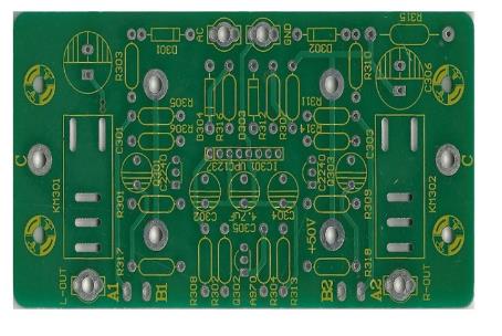
There is a deep understanding of the importance of the stability of electronic PCB products. Buying electronic products does not want to buy a smart bracelet that needs to be calibrated every day, nor does it want to buy an electronic product that is prone to crashes. Once this happens, Among the electronic products purchased, then, the fate of this electronic product may be reaching the end, and the product in hand may be ashes in the corner of the drawer or become useless.
Electronic products will produce abnormalities that are affected by many factors, such as ESD, EMI, or design defects in principle. So how to design an electronic product with stable performance, you need to pay attention to several aspects.
First, eliminate design defects in principle
This part is very important, especially when the external interface circuit requires low-power design, you should pay more attention to it. For example, a button is usually designed to be pulled up to VDD during normal design, but in low-power design, It needs to be connected to GND and pulled up to VDD when there is an action.

In addition to designing schematic diagrams for product characteristics, it also helps in the selection of components. Such as packaging, power consumption, working environment, etc. all need to be considered.
Second, reasonable layout
This part is a technical or artistic problem. Reasonable layout requires reasonable arrangement of the connections, locations and wiring of the various units in the system equipment. What needs attention is the separation of high-speed and vulgarity, the separation of analog and digital, and the source of interference is far away from the core components. Note that the high-frequency connection should be as short as possible, and the grounding resistance should be as small as possible. I believe this is an unfinished book for EE. This reminds me of a sentence: A PCB board with excellent performance is a good product, and its layout is a work of art.
Third, do a good job of shielding
The vulgar PCB that is usually designed can operate normally without any shielding system. But if you disassemble and look at the mobile phone, handheld or other communication equipment, you find that the key radio frequency circuit is often hidden under the Faraday cage. This is a method of shielding.
As an effective way to suppress radiated interference, shielding is often used in severe EMI disaster areas, but it is not as long as shielding is used to solve EMI problems. It is accompanied by grounding problems. Only when shielding and grounding are used together can shielding be used. Maximum effect. If it is not grounded, then this electric cage may become a panel antenna that collects energy and emits even greater energy EMI.
There are electrical shielding, magnetic shielding and electromagnetic shielding. Different shielding technologies use different shielding design methods:
Electric shielding usually chooses copper-aluminum alloy as the shielding material. In high-frequency shielding, it is necessary to plate the surface of the shield with silver. For its shape, a box shape is generally selected to obtain good shielding performance. Try not to open holes on the shield to avoid leakage of electric field energy. If holes have to be opened for some reason (heat dissipation), the number of openings should be as small as possible and the opening area should be as small as possible.
Everyone who has studied electromagnetic field knows that the shielding effect of eddy current is very small in low-frequency magnetic field, and high permeability materials are usually needed for shielding. The thicker the shielding shell and the higher the magnetic permeability, the better the magnetic shielding effect. Magnetic shielding adopts steel plate as shielding cover, and double-layer shielding can be used if necessary.
The same method can be used for electromagnetic shielding and electrical shielding, and suitable conductive gaskets, comb-shaped reeds, and shielding display windows can be selected according to the actual situation to achieve electromagnetic sealing.
For shielding, there are usually the following steps:
Fourth, do a good job of isolation
For ordinary IO interfaces, if you need to detect external voltage or switch status, you can connect directly. However, in order to prevent overcurrent or overvoltage, the IO port needs to be protected. At this time, the IO port isolation method can be used. Transistor and optocoupler It is a good method to adopt, and there are methods such as transformer isolation and component isolation.
Fifth, good grounding
Regarding the grounding technology, there has been a very detailed description in the previous small article. For details, see: Grounding technology that electronic design has to say
The above content is a summary of experience in designing and debugging circuits. With the development of technology, I believe that there will be more methods for PCB design, which also records the growth process of every EE.