Generally, when considering a multi-layer circuit board PCB design, a combination of circuit board racks or game platforms in a server environment is often thought of. But what if a typical rigid board is not suitable for the physical chassis used in a multilayer board? Are you willing to pay extra for the use of flexible circuit boards? What if the advantages of the two can be combined?
The advantages and properties of rigid-flexible combination and how to better meet the PCB design requirements of multi-layer boards.
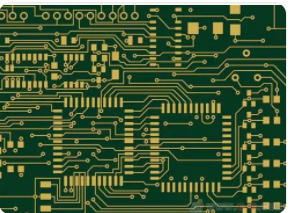
What is rigid flexible PCB?
In the standard multi-layer circuit board PCB design, the circuit board concept is used to divide different functional circuits into smaller circuit boards, and various interconnections are used to put the system into a single housing.
The standard method for this problem is that the reliability of the interconnection cannot be guaranteed (especially after considering electromagnetic interference/electromagnetic compatibility issues). Standard card edge connectors have good conductivity and meet our size requirements and do not always exist; the best alternative is cables, but cables are not practical, and they cannot meet the space requirements of the chassis.
If the multi-layer circuit board design requires us to interconnect several rigid boards with a compact enclosure, with high-level connections and high-speed connections, the combination of rigid-flexible combinations is the best solution.
What is a rigid combination? Simply put, two or more rigid boards are electrically connected by a flexible part.
A single flexible layer usually consists of the following materials:

Flexible polyimide core;
Conductive copper layer;
Adhesive
The conductive copper layer is sandwiched on both sides with a flexible polyimide adhesive. The polyimide layer and the adhesive layer are generally considered to be a unit (called a cover layer), which can be laminated on the copper layer by heat and pressure. Multiple flexible layers can be used in any given design.
The rigid part is added to the flexible layer through the rigid layer of standard PCB material:
Inject glass fiber prepreg with resin, it will flow and bond when heated;
Non-conductive glass fiber base layer (usually FR-4);
Traditional green solder mask;
Screen printing marks and identification information
The flexible polyimide layer and the conductive copper layer are usually continuous on the entire board (including the rigid layer and the flexible layer). However, some designs limit the amount of flexible polyimide used to fill the rigid layer portion with prepreg.
In terms of design, the rigid-flex combination is considered a folded circuit board. This reduces the total number of interconnections required in the system and avoids manual steps such as soldering flat ribbon cables to rigid boards.
Common rigid and soft combination configuration
Standard configuration: flexible layer in the center of the symmetrical structure stack. It usually uses a uniform number of layers similar to standard multi-layer PCB designs.
Odd-numbered layer count configuration: Although not common in traditional PCB design, odd-numbered layer counts provide both sides of the EMI shielding flexible layer on both sides to meet strip impedance control and electromagnetic compatibility requirements.
Asymmetrical configuration: If the flexible layer is not in the center of the stack, it is considered an asymmetrical configuration. Sometimes the requirements for impedance and dielectric thickness vary greatly, leading to a "heavy top" design. At other times, the blind hole aspect ratio can be reduced by the asymmetric structure. Due to the easy deformation and twisting of the design, it may be necessary to press the clamp.
Blind vias and buried vias: Rigid-flex circuit supports connecting external blind via PCB layers to one or more inner layers without passing through the entire board; buried vias connect one or more inner layers without passing through outer layers. The composite via structure usually requires an asymmetric structure when processing the flexible layer.
Shielding flexible layer: Special shielding film (such as Tatsuta and APlus) laminated on the flexible layer. A special cover opening with conductive adhesive brings the shielding film to the ground. These films can shield flexible areas without significantly increasing the thickness.
There are many different configurations for rigid and soft combinations. The number of layers between rigid and flexible components does not need to be matched, and the PCB design can be fully customized to fit the sealed enclosure; just ensure that the design meets the quality standards specified in IPC 2223C.
Summarize
Rigid-Flexible bonding helps to meet complex geometric or electromagnetic interference requirements, allowing flexible circuits or strong rigid boards to be used as much as possible to minimize manufacturing and assembly costs.
Since rigid design can usually handle complex 3D requirements, it is necessary to have a powerful PCB design software that supports the overall design method to bridge the gap between the electromechanical fields.