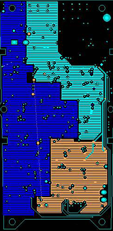
In fact, the work of high-speed PCB design needs to face many different product directions. Although some basic technologies are universal, there are still many industry-specific technical differences, because the core design requirements of each field are different. For example, consumer products highlight the cost-performance ratio; on the contrary, the military and industrial fields require absolute reliability; and the data and communications fields require extreme product performance... This all raises the design rules and the direction of technology research and development. Very different requirements.
If we talk about the core key points of relatively general high-speed PCB design, I think we must pay attention to the following aspects:
1: First is the design of the power circuit
The power supply is the basis for the stable operation of an electronic product. Although most of the time the technical challenge of power supply design is not the most challenging, once the problem of operational stability occurs, it is actually related to the power supply in many cases.
The focus of power supply design mainly lies in the optimization of the functional design of the power module, the improvement of conversion efficiency, and the design of power channels, etc., which must be carried out in accordance with the corresponding technical indicators and rules. For sensitive power supplies or power supplies with large currents, PI simulation is also required. Improve the performance of DC voltage drop, dynamic impedance and noise.

2: Design of high-speed parallel signals
The most common ones are DDR3, DDR4 and other circuits. Especially for the Memory Down (onboard memory) design, special attention is needed. While strictly implementing the original Layout Guide, it is best to optimize the layout design through simulation analysis. To ensure the design quality of high-speed signals.
There are many other types of parallel signal designs. Generally, the absolute length and the relative equal length are controlled according to the corresponding chip design rules. At the same time, the control of the number of vias, signal span division, and crosstalk can satisfy most designs. Require.
3: High-speed serial signal design
In recent years, high-speed serial signals have developed very rapidly. Many traditional parallel bus interfaces are gradually being replaced by serial buses. For example, the most typical IDE parallel hard disk data interface is replaced by SATA serial data interface. I believe that high-speed The application of serial signal will become more and more extensive.
At present, the most common PCIE high-speed channels, as well as SATA, SAS, LVDS, USB3.0 high-speed channels, and high-speed optical network channels, have generally increased the signal speed to the level of 5G, 8G, 10G, 28G and even 56Gbps, so strict Design according to the corresponding high-speed design rules, and at the same time do a good job in signal integrity analysis and optimization, otherwise it will be prone to signal quality problems.
4: There are many other key technical points that need to be paid attention to, such as analog signal design, radio frequency signal, digital-analog mixing, and DFM, DFX, EMC design attention points, etc., each direction has a series of rules and requirements. Interested friends can do in-depth study and research, and I will not do it here.
The ins and outs of high-speed PCB design
This is more difficult to say clearly in a few words. Because any professional field has its own set of work processes and rules system, this is a very complex technical and management system engineering. If you want to have a deep understanding of a certain industry, you can only really figure it out if you personally enter the industry and spend a few years working hard. And even in the same industry, but in different technical fields, there are also big differences.
As the saying goes, interlacing is like a mountain. Even if you have worked in a specific field in the same industry for many years, if you switch to another field, it is possible that your previous work experience will be completely cleared. For example, if you jump from the field of low-end consumer product design to the field of military and communication product design, the previous work experience may be very limited because the design rules are completely different from the knowledge system. This is actually the difference between the PCB industry and the circle, so it is not only the choice of the PCB industry, but it is actually more important to pay attention to the difference and choice of the circle.
How does the PCB design team solve technical challenges from multiple perspectives?
To solve the technical challenges of high-speed PCB design, we need to start from multiple aspects. The core technical points have been mentioned above and will not be repeated. I will briefly summarize the corresponding solutions here:
1: SI high-speed signal integrity analysis: to analyze signal integrity and guide the optimization of PCB design
2: PI power integrity analysis: to improve power supply channel design, optimize decoupling capacitor design, etc.
3: DFM manufacturability analysis: optimize product manufacturing process performance, reduce cost and improve quality
4: DFA analysis: analyze and optimize the performance of SMT patching, maintenance, and testing to improve production efficiency
5: EMC analysis: focus on optimizing EMI and ESD performance to ensure compliance with technical certification indicators
6: Other analysis: such as purchase cost, structural heat dissipation, life and reliability optimization, etc.