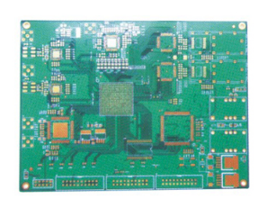
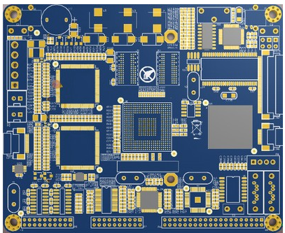
1. What are the common problems in PCBA processing?
PCBA processing manufacturers usually have more common problems in the process of PCBA processing and production.
1. Short circuit
Refers to the phenomenon of joining between two independent adjacent solder joints after soldering. The cause is that the solder joints are too close, the parts are arranged improperly, the soldering direction is incorrect, the soldering speed is too fast, the flux coating is insufficient, and Poor solderability of parts, poor solder paste coating, excessive solder paste, etc.
2. Empty welding
There is no tin on the tin trench, and the parts and the substrate are not welded together. The reasons for this situation are unclean welding trenches, high feet, poor solderability of parts, excessive parts, improper dispensing operations, so that the glue overflows in the welding trenches. The first class will cause empty welding. The PAD parts of the empty welding are mostly bright and smooth.
3. False welding
There is tin between the foot of the part and the welding trench, but it is actually not completely caught by the tin. Most of the reason is that rosin is contained in the solder joints or caused by it.

4. Cold welding
Also called undissolved tin, it is caused by insufficient flow soldering temperature or too short flow soldering time. Such a shortcoming can be improved by secondary flow soldering. The surface of the solder paste at cold solder joints is dark and mostly powdery.
5. Parts fall off
After the soldering operation, the parts are not in the proper position. The reasons for this are improper selection of glue material or improper glue dispensing operation, incomplete maturation of the glue material, excessive tin wave and too slow soldering speed, etc.
6. Missing parts
Parts that should be installed but not installed.
7. Damaged
The appearance of the parts is obviously broken, material defects, or process bumps are caused, or the parts are cracked during the soldering process. Insufficient preheating of parts and substrates, too fast cooling rate after soldering, etc., all contribute to the tendency of parts to crack.
8. Denudation
This phenomenon mostly occurs on passive parts. It is caused by poor plating treatment on the terminal part of the part. Therefore, when passing through the tin wave, the plating layer melts into the tin bath, causing the structure of the terminal to be damaged, and the solder does not adhere. Good, and higher temperature and longer soldering time will make the bad parts more serious. In addition, the general flow welding temperature is lower than wave welding, but the time is longer. Therefore, if the parts are not good, it will often cause erosion. The solution is to change the parts and control the flow welding temperature and time appropriately. The solder paste with silver content can inhibit the dissolution of the end of the part, and the operation is much more convenient than the change of the solder composition of wave soldering.
9. Tin Tip
The surface of the solder joints is not a smooth continuous surface, but has sharp protrusions. The possible causes of this are excessive soldering speed and insufficient flux coating.
10. Shaoxi
The amount of tin in the welded parts or parts feet is too small.
11. Tin ball (bead)
The amount of tin is spherical, on the PCB, part, or part foot. Poor quality of solder paste or storage for too long, unclean PCB, improper solder paste coating operation, and too long operation time of solder paste coating, preheating, and flow soldering are all likely to cause solder balls (beads).
12. Open circuit
The line should be turned on but not turned on.
13. Tombstone effect
This phenomenon is also a kind of open circuit, which is easy to occur on CHIP parts. The cause of this phenomenon is that during the soldering process, due to the different tensile forces between the different solder joints of the parts, one end of the part is tilted, and the tensile force at both ends is different. So the difference is related to the difference in the amount of solder paste, solderability and tin melting time.
14. Wick effect
This mostly occurs on PLCC parts. The reason for this is that the temperature of the part feet rises higher and faster during flow soldering, or the solder cut has poor solderability, which causes the solder paste to rise along the part feet after the solder paste melts., Resulting in insufficient solder joints. In addition, insufficient preheating or no preheating, and easier flow of solder paste, etc., will promote this phenomenon.
15. CHIP parts turn white
In the SMT chip processing process, the marking surface of the part value is soldered on the PCB by the front and back, and the part value cannot be seen but the part value is correct, which will not affect the function.
16. Reverse polarity/direction
The component is not placed in the specified orientation.
17. Shift
18. Too much or not enough glue:
19. Side Standing
2. General rules for the operation of PCBA boards and components
Incorrect operation will immediately cause damage to components and PCBA boards (such as cracking, chipping, breaking of components and connectors, bending or breaking of terminal leads, and scratching of the surface of the circuit board and conductor pads) ). Such physical hazards can destroy the entire PCBA or various components on it. In order to ensure the completeness and consistency of the production process during all production periods, great care must be taken in the qualification test. Therefore, the following general operating guidelines for the general rules of PCBA board and components are proposed.
1. Keep the workbench clean and tidy. There should not be any food or drink in the work area, smoking and placing cigarettes and ashtrays are prohibited.
2. Reduce the operation steps of PCBA and components to a minimum to prevent danger. In assembly areas where gloves must be used, soiled gloves will cause contamination, so gloves must be replaced frequently when necessary.
3. As a general rule, the surface to be welded should not be taken with bare hands or fingers, because the grease secreted by human hands will reduce the weldability.
4. Do not use skin-protecting oils to coat hands or various silicone-containing detergents, as they can cause problems in solderability and adhesion of conformal coatings. A specially formulated detergent for PCB soldering surface is available.
5. PCBA must not be stacked, otherwise physical damage will occur. Special brackets should be provided on the assembly work surface.
6. Components and PCBA boards that are sensitive to EOS/ESD must be marked with appropriate EOS/ESD marks. Numerous sensitive PCBAs should also have relevant marks themselves, and these marks are usually on a board edge connector. In order to prevent ESD and EOS from endangering sensitive components, all operations, assembly and testing must be completed on a workbench that can control static electricity.
Impurity contamination caused by operation without some form of protective measures will cause problems in circuit board welding and conformal coating. The salt and grease secreted by the human body and the unauthorized use of hand oil are both It is a typical pollution source. The usual cleaning process generally cannot eliminate the above-mentioned contaminants. To solve such problems, special measures must be taken to prevent the emergence of such pollution sources.