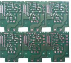
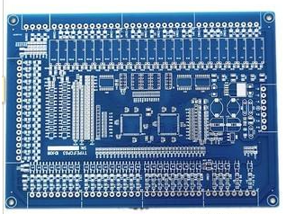
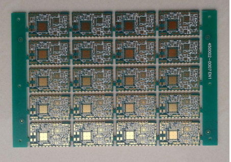
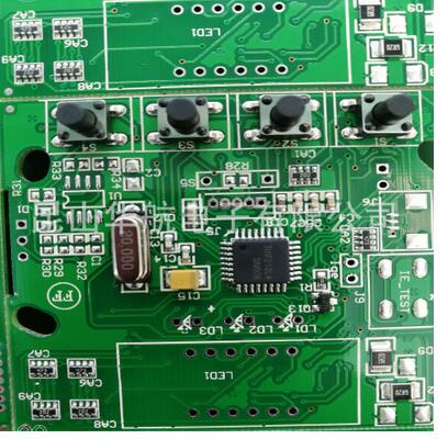
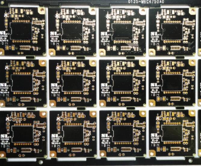
PCBA appearance quality inspection standards describe the materials, methods and qualification requirements used to produce high-quality solder joints and PCBA. No matter what other feasible methods are used, it must be able to produce complete solder joints that meet the qualification requirements described in this standard. This standard is applicable to quality inspection personnel and process personnel at trial production and production sites when conducting PCBA appearance inspection. This standard applies to most PCBA products.
PCBA appearance quality inspection standard
Eligibility Judgment During the implementation of this standard, there are three judgment states: "best", "qualified" and "unqualified".
Optimal: It is an idealized state, which is not always achieved, nor is it required to be achieved. But it is the goal pursued by the craft department.
Qualified: It is not optimal, but it can maintain the integrity and reliability of the PCBA under the environment in which it is used.

For some changes in the process, the qualification requirements are slightly higher than the minimum requirements of the final product. In order to allow certain changes in the process, the qualification requirements are slightly higher than the minimum requirements of the final product.
Unqualified: It is not enough to guarantee the shape, fit and function requirements of the PCBA in the final use environment. It should be disposed of (rework, repair or scrap) according to design requirements, use requirements and user requirements.
Many examples (illustrations) of this standard show unqualified situations that are a bit exaggerated. This is done deliberately for the convenience of explanation.
The use of this standard requires special attention to the subject of each section to avoid misunderstandings.
Automatic inspection technology (AIT) can effectively replace manual appearance inspection and can be used as a supplement to automatic testing equipment. Many of the features described in this standard can be verified by the AIT system.
How to use this standard
This standard can be used in conjunction with the standard J-STD-001B "PCBA Soldering Quality Requirements" jointly formulated by IPC and EIA. J-STD-001B establishes the minimum qualification requirements for PCB soldering. This standard is a similar document and supplement. It provides a graphical description of J-STD-001B. This standard also includes requirements for operation, mechanical assembly, and other process requirements.
This standard can be used as an independent application document for inspection, but it does not specify the frequency of on-site process inspection or the frequency of final product inspection. It also does not specify the number of allowable "process problem warnings" (respectively classified as "qualified" and "unqualified"), nor does it specify the number of defects that are allowed to be repaired/reworked. These regulations can be found in J-STD-001B.
If quality engineers and process engineers need to arbitrate on some of the inspected content on site, they should use J-STD-001B to further understand the details of welding requirements.
Size check
Except for the purpose of arbitration, this standard does not provide actual dimensional data (ie, specific component installation and weld size, percentage determination value).
PCBA appearance quality inspection standard
Amplification aids and lighting
Because it is an appearance inspection, when performing PCBA inspection, optical magnification auxiliary devices can be used for some individual technical content.
The accuracy of the magnification auxiliary device is the selected magnification
15% of the number (that is, ±15% or 30% of the selected magnification). Amplification aids and inspection lighting should be compatible with the size of the product being processed. The magnification used to inspect the solder joints is based on the minimum width of the pad used by the inspected device. When the quality engineer requires a magnification inspection, the following magnifications can be applied:
The arbitration situation should only be used to identify products that fail the inspection. For PCBAs with various pad widths, a larger magnification can be used to inspect the entire PCBA.
Circuit board orientation
In the full text of this standard, the following terms are used to determine the PCB surface:
Main surface: the side of the package and interconnection structure. This side is specified in the layout plan (usually this side contains the most complex or most components. This side is sometimes called "components" in through-hole insertion technology. Device surface").
Secondary side: The side of the package and interconnect structure, which is the opposite side of the main side. (This surface is sometimes referred to as the "welded surface" in through-hole insertion technology).
Electrical spacing: Whenever possible, the spacing between conductors on different levels should be as large as possible. In this standard, the minimum distance between conductors, between conductive patterns, and between conductive materials (such as conductive marks or mounting hardware) and conductors is referred to as the "minimum electrical distance, and is consistent with the corporate standard "Printed Circuit Board (PCB) The "Design Code" complies with the requirements, and it is stipulated in the general layout plan.