Differences about HDI PCB
High-density interconnect printed circuit boards (HDI PCBs) have enabled technological advances in electronic technology. They are called various names: Sequence Build (SBU), Microvia Process (MVP) and Build Up Multilayer (BUM) boards, to name a few. In the end, IPC (Electronic Industries Federation) adopted the HDI term, which is a consistent term for countries and the PCB manufacturer industry.
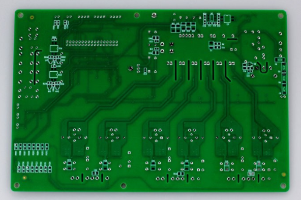
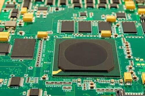
HDI PCB has the technical characteristics of extremely high-density wiring interconnection, which can realize high-density components. These attributes contribute to the high performance and lightweight of HDI boards, making them ideal for today's equipment. HDI PCB is the perfect solution for electronic technology to shrink the size, including notebook computers, tablet computers, smart phones and other core components of technological miracles, and even wearable technologies such as fitness bands and virtual reality devices.
Why use HDI PCB?
HDI boards have many technical and physical advantages compared to traditional through-hole or even standard surface mount technology (SMT) boards:
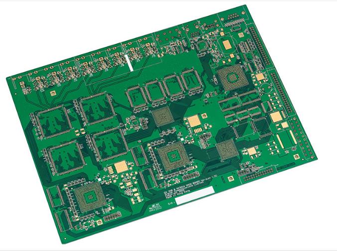
Size-Through pure technical characteristics, HDI boards can accommodate more connections on printed circuit boards of the same size to obtain more dense PCBs with fewer layers. Design advantages-By increasing the board capacity, HDI provides designers with greater flexibility and helps speed up signal processing. Reliability-IPC research refers to the excellent reliability (TH) provided by the small blind holes on the through holes due to the greatly reduced aspect ratio (AR) of the through holes. HDI is actually the only option, which includes more complex and dense packages, such as packages with high pin counts and very low pitch. The demand for small circuit boards-manufacturers need smaller and lighter circuit boards and more features. Non-HDI panels require more space and weight, making HDI technology an obvious choice. Function-Using HDI, multiple traditional PCBs can be integrated into one HDI PCB. Signal integrity-Improving electrical performance and improving signal integrity requirements are attributes provided by HDI technology. HDI board design requirements
HDI technology brings its own characteristics to a set of specific design issues:

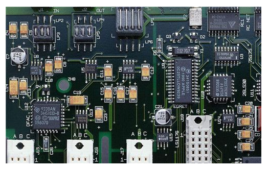
Material selection-All PCB designs consider material and component selection, but for HDI, there are unique manufacturing constraints. The selected material will affect the electrical performance of the signal trace, and of course the cost of the final product. Micro-via stacking-an effective design can take advantage of HDI to stack micro-vias instead of staggering. Every Layer Interconnect (ELIC)-This technology, now popular in smartphone structures, provides smaller spacing, eliminates mechanical holes in the board, and takes up space. Blind areas and buried holes. The asymmetrical design of the stack will cause uneven pressure and cause the circuit board to warp. Component layout-The density of HDI technology requires close attention to placement to ensure the feasibility of soldering, installation and maintenance of the circuit board. By allowing the maximum space tolerance while still utilizing the available density, this will facilitate any necessary rework. Track uniformity and minimum line width. These factors are important considerations to avoid open circuit and short circuit conditions.
When formalizing HDI design, the most common problems are still cost and quality, which are the main concerns of consumers when buying. A device containing a circuit board.
Thoughts when considering using HDI
There are other points to consider before implementing HDI in PCB design:
Skill Combination-Planning PCB functions is completely different from HDI PCB designers. Before sending the PCB to the manufacturer, high density, layer considerations, and manufacturing complexity are all factors that need to be planned. Design issues after the start of manufacturing work are costly and can lead to a complete redesign and scrapping of any circuit boards that have already been produced. Planning-Significant changes in PCB layout or functions in HDI boards are very difficult, making an accurate and error-free design process critical to cost-effective manufacturing. Careful planning and design will promote the successful production and function of the circuit board and keep the project within budget.
Each of these points emphasizes the need to consider design for manufacturing (DFM) tools and processes. It is also important to seek manufacturer’s recommendations and design recommendations, which will actually produce HDI boards before manufacturing begins.