PCB errors are not uncommon
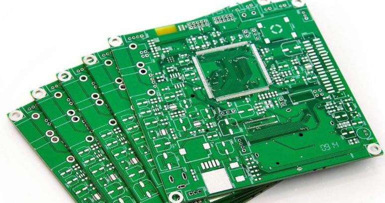
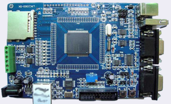
Printed circuit boards (PCBs) are becoming more and more complex and at the same time becoming more and more important to technology. PCBs are not only the basic components of computers and high-tech communication equipment, but also can be used in various cars, smart phones, lighting systems and even children's toys.
With the increasing complexity and miniaturization of printed circuit boards, design engineers face the challenge of keeping up with the development of available materials, design and layout software, and manufacturing capabilities. No wonder there are many opportunities to make mistakes in PCB development.
When avoiding common PCB design errors, it is important to look for:
Layout issues, such as missing traces or vias, incorrect trace or pad size, and noise generation.
Schematic errors that cause performance problems or failures of all functions. Because certain PCBs and multilayer boards require a smaller footprint, it becomes easier to generate layouts that are difficult during manufacturing or during testing.

Failure due to environmental issues. Designers need to understand the expected environment facing their designs and plan materials and layouts accordingly. Every situation to which the final product will be exposed should be assessed for potential PCB failures or conditional issues.
Do not use available tools. Electronic design automation (EDA) tools are widely available, but they are not all equal. Evaluate the available applications to determine which is best for the PCB to be designed. The design tool can improve the layout design and generate all the files needed to make the circuit board.
No review process is required. The lack of communication between the electronic engineer and the PCB designer (when they are different technicians) can cause the circuit board to fail to operate according to the engineer's plan.
Test Plan. The prototype board can pass the initial test of basic functions, but it may malfunction when the circuit board is put into production and installed in the final product. It is now difficult to find that the PCB performs poorly (or not at all) in certain settings. At this time, the cost of rework and product recalls becomes very expensive.
missing file. It is not common for manufacturers to return to designers who are incomplete documents or documents that may not be clearly marked/named in order to identify the documents used for manufacturing. This can cause circuit board failure or manufacturing delays.
Lack of familiarity with manufacturing requirements. If the designer does not understand the manufacturing process, even the most carefully designed circuit with the most advanced technology design may not be effectively manufactured. This may include dimensional tolerances beyond the necessary range, resulting in manufacturing complexity, thereby increasing costs and even changing the floor space of the resulting board.
Avoid common PCB design mistakes
By implementing some standard procedures and best practices, many common PCB errors can be easily avoided or at least reduced:
Even the most savvy design engineer can make mistakes-usually errors that the second designer can easily spot. Initiating a peer review can help catch at least some of these design errors, or at least raise issues that may indicate design flaws or lack of notes and documentation that could cause manufacturing delays.
Use complex tools and PCB layouts available for design, and learn to use them effectively. Training in the proper use of design tools can avoid unintentional errors in layout or manufacturing specifications. Don't underestimate the value of thorough training.
Manufacturing design. The available layout design software application has developed by leaps and bounds in recent years, but it can only be as good as software developers. The final design generated by the layout design software can provide a seemingly viable PCB, but when it reaches the manufacturer, there may be problems that make the design difficult or even impossible to manufacture. To avoid such problems, implement procedures that utilize design-to-manufacture (DFM) software before sending the design for use in manufacturing prototypes or final products. Such applications can detect possible manufacturing issues, missing files, etc.
Use saved templates. By setting up standard templates that all designers can access, the design can be completed in a more timely manner, reducing the worry about omissions and obvious errors.
Collaborate with manufacturers. By establishing good practice relationships and consistent communication relationships with PCB manufacturers, design engineers can solve problem areas in the shortest possible time, and have the least impact on the cost of the circuit board due to early detection.