PCB is the abbreviation of English (Printed Circuie Board) printed circuit board. Generally, the conductive pattern made of printed circuits, printed components or a combination of the two on the insulating material according to a predetermined design is called a printed circuit. The conductive pattern that provides electrical connections between components on an insulating substrate is called a printed circuit. In this way, the printed circuit or the finished board of the printed circuit is called a printed circuit board, also called a printed circuit board or a printed circuit board.
PCB can almost be seen in electronic equipment can not be separated from it, as small as electronic watches, calculators, general-purpose computers, as large as computers, communication electronic equipment, military weapon systems, as long as there are electronic components such as integrated circuits, between them PCB is used for electrical interconnection. It provides mechanical support for the fixed assembly of various electronic components such as integrated circuits, realizes wiring and electrical connection or electrical insulation between various electronic components such as integrated circuits, and provides required electrical characteristics such as characteristic impedance. At the same time, it provides solder mask graphics for automatic soldering; provides identification characters and graphics for component insertion, inspection, and maintenance.

How is PCB made? When we open the keyboard of a general-purpose computer, we can see a piece of soft film (flexible insulating substrate), printed with silver-white (silver paste) conductive patterns and healthy bit patterns. Because the general screen printing method obtains this kind of pattern, we call this kind of printed circuit board a flexible silver paste printed circuit board. The printed circuit boards on the various computer motherboards, graphics cards, network cards, modems, sound cards and household appliances that we saw in the Computer City were different. The substrate used in it is made of paper base (usually used for single-sided) or glass cloth base (usually used for double-sided and multilayer), pre-impregnated with phenolic or epoxy resin, and the surface layer is laminated with copper-clad film on one or both sides and then laminated to cure Become. This kind of circuit board copper clad sheet material, we call it rigid board. And then make a printed circuit board, we call it a rigid printed circuit board. We call single-sided printed circuit boards with printed circuit patterns on one side, and printed circuit boards on both sides with printed circuit patterns on both sides. The printed circuit boards formed by double-sided interconnection through hole metallization are called double-sided boards. If a printed circuit board with one double-sided as the inner layer, two single-sided as the outer layer, or two double-sided as the inner layer and two single-sided as the outer layer of the printed circuit board, the positioning system and the insulating bonding material are alternately together and The printed circuit board with the conductive pattern interconnected according to the design requirements becomes a four-layer or six-layer printed circuit board, also called a multilayer printed circuit board. There are now more than 100 layers of practical printed circuit boards.
PCB production process is more complicated, it involves a wide range of processes, from simple mechanical processing to complex mechanical processing, there are common chemical reactions, photochemical, electrochemical, thermochemical and other processes, computer-aided design CAM and other aspects of knowledge. Moreover, there are many process problems in the production process and new problems will be encountered from time to time. Some of the problems disappear without finding out the cause. Because the production process is a non-continuous assembly line form, any problem in any link will cause the entire line to stop production. Or as a result of a large number of scraps, if printed circuit boards are scrapped, they cannot be recycled and reused. The work pressure of process engineers is relatively high, so many engineers have left the industry and turned to printed circuit board equipment or material vendors to do sales and technical services. .
In order to further understand the PCB, it is necessary to understand the production process of the usual single-sided, double-sided printed circuit board and ordinary multilayer board, in order to deepen the understanding of it.
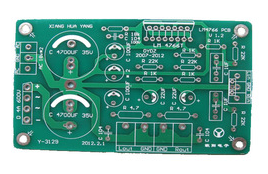
Single-sided rigid printed circuit board: - single-sided copper clad laminate - blanking - (brushing, drying) - drilling or punching - screen printing circuit anti-etching pattern or using dry film - curing inspection and repairing board - etching copper - removing corrosion Printing, drying - brushing, drying - screen printing solder mask graphics (commonly used green oil), UV curing - screen printing character marking graphics, UV curing - preheating, punching and shape - electrical opening, short circuit test - brushing, drying - Pre-coated anti-oxidant (dry) or spray tin and hot air leveling - inspection and packaging - finished products leave the factory.
Double-sided rigid printed circuit board: -Double-sided copper clad laminate - blanking - stacking board - CNC drilling through holes - inspection, deburring and brushing - chemical plating (through hole metallization) - (full board electroplating of thin copper) - inspection Brushing - screen printing negative circuit patterns, curing (dry film or wet film, exposure, development) - inspection, repairing - circuit pattern plating - tin electroplating (anti-corrosive nickel/gold) - removing printing material (photosensitive film) - etching Copper-(removing tin)-cleaning and scrubbing-screen printing solder mask graphics commonly used thermal curing green oil (photosensitive dry film or wet film, exposure, development, thermal curing, commonly used photosensitive thermal curing green oil)-cleaning, drying-screen printing Mark character graphics, curing-(spray tin or organic solder mask)-shape processing-cleaning, drying-electrical on-off test-inspect packaging-the finished product leaves the factory.
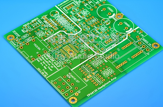
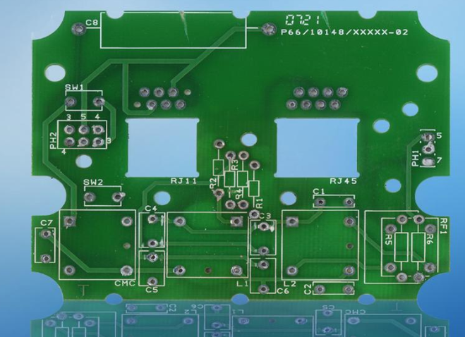
Common computer boards are basically double-sided printed circuit boards based on epoxy resin glass cloth. One side is for inserting components and the other side is for component pin soldering. It can be seen that the solder joints are very regular. The components of these solder joints The discrete soldering surface of the foot is called a pad. Why are other copper wire patterns not tinned? Because in addition to the soldering pads and other parts, the surface of the remaining parts has a solder mask that is resistant to wave soldering. Most of the solder mask on the surface is green, and a few use yellow, black, blue, etc., so solder mask oil is often called green oil in the PCB industry. Its function is to prevent bridging phenomenon during wave soldering, improve soldering quality and save solder. It is also a permanent protective layer for printed boards, which can prevent moisture, corrosion, mildew and mechanical scratches. From the outside, the smooth and bright green solder mask is a green oil that is photosensitive and thermally cured for the film on the board. Not only does the appearance look better, it is also important that the pads are more accurate, which improves the reliability of the solder joints.