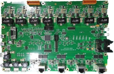
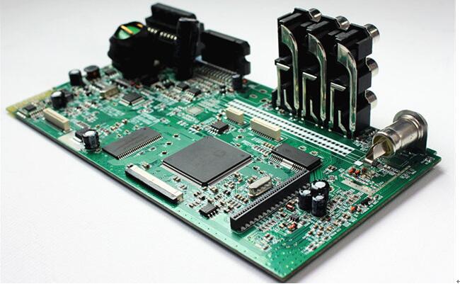
The general surface treatments of PCB circuit boards include tin spraying, OSP, and gold immersion. The "surface" here refers to the connection points on the PCB that provide electrical connections between electronic components or other systems and the circuit of the PCB, such as A connection point for a pad or contact connection. The solderability of bare copper itself is very good, but it is easy to oxidize when exposed to the air, and it is easy to be contaminated. This is why the PCB must be surface treated.
1. Spray tin (HASL)
Where perforated devices dominate, wave soldering is the best soldering method. The use of hot-air solder leveling (HASL, Hot-air solder leveling) surface treatment technology is sufficient to meet the process requirements of wave soldering. Of course, for the occasions that require high joint strength (especially contact connection), electroplating of nickel/gold is often used. . HASL is the main surface treatment technology used worldwide, but there are three main driving forces that drive the electronics industry to consider alternative technologies for HASL: cost, new process requirements and lead-free requirements.

From a cost point of view, many electronic components such as mobile communications and personal computers are becoming popular consumer goods. Only by selling at cost or lower prices can we be invincible in the fierce competitive environment. After the development of assembly technology to SMT, PCB pads require screen printing and reflow soldering processes during the assembly process. In the case of SMA, the PCB surface treatment process still used HASL technology initially, but with the continuous shrinking of SMT devices, the pads and stencil openings have also become smaller, and the drawbacks of HASL technology have gradually been exposed. The pads processed by HASL technology are not flat enough, and the coplanarity cannot meet the process requirements of fine-pitch pads. Environmental concerns usually focus on the potential impact of lead on the environment.
2. Organic Solderability Protective Layer (OSP)
Organic solderability preservative (OSP, Organic solderability preservative) is an organic coating used to prevent copper from oxidizing before soldering, that is, to protect the solderability of PCB pads from damage.
After the PCB surface is treated with OSP, a thin organic compound is formed on the surface of the copper to protect the copper from oxidation. The thickness of Benzotriazoles OSP is generally 100 A°, while the thickness of Imidazoles OSP is thicker, generally 400 A°. OSP film is transparent, it is not easy to distinguish its existence with the naked eye, and it is difficult to detect. During the assembly process (reflow soldering), the OSP is easily melted into the solder paste or acidic Flux, and at the same time the active copper surface is exposed, and finally Sn/Cu intermetallic compounds are formed between the components and the pads. Therefore, OSP has very good characteristics when used to treat the welding surface. OSP does not have the problem of lead pollution, so it is environmentally friendly.
Limitations of OSP:
1. . Since OSP is transparent and colorless, it is difficult to inspect, and it is difficult to distinguish whether the PCB has been coated with OSP.
2. OSP itself is insulated, it does not conduct electricity. The OSP of Benzotriazoles is relatively thin and may not affect the electrical test, but for the OSP of Imidazoles, the protective film formed is relatively thick, which will affect the electrical test. OSP can't be used to handle electrical contact surfaces, such as keyboard surfaces for keys.
3. During the welding process of OSP, stronger Flux is needed, otherwise the protective film cannot be eliminated, which will lead to welding defects.
4. During the storage process, the surface of the OSP should not be exposed to acidic substances, and the temperature should not be too high, otherwise the OSP will volatilize.
3. Immersion gold (ENIG)
ENIG's protection mechanism:
Ni/Au is plated on the copper surface by chemical method. The deposition thickness of the inner layer of Ni is generally 120 to 240 μin (about 3 to 6 μm), and the deposition thickness of the outer layer of Au is relatively thin, generally 2 to 4 μinch (0.05 to 0.1 μm). Ni forms a barrier layer between solder and copper. During soldering, the Au on the outside will quickly melt into the solder, and the solder and Ni will form a Ni/Sn intermetallic compound. The gold plating on the outside is to prevent Ni oxidation or passivation during storage, so the gold plating layer should be dense enough and the thickness should not be too thin.
Immersion gold: In this process, the purpose is to deposit a thin and continuous gold protective layer. The thickness of the main gold should not be too thick, otherwise the solder joints will become very brittle, which will seriously affect the reliability of welding. Like nickel plating, immersion gold has a high working temperature and a long time. During the dipping process, a displacement reaction will occur-on the surface of nickel, gold replaces nickel, but when the displacement reaches a certain level, the displacement reaction will automatically stop. Gold has high strength, abrasion resistance, high temperature resistance, and is not easy to oxidize, so it can prevent nickel from oxidation or passivation, and is suitable for working in high-strength applications.
The PCB surface treated by ENIG is very flat and has good coplanarity, which is the only one used for the contact surface of the button. Secondly, ENIG has excellent solderability, gold will quickly melt into the molten solder, thereby exposing fresh Ni.
Limitations of ENIG:
ENIG's process is more complicated, and if you want to achieve good results, you must strictly control the process parameters. The most troublesome thing is that the ENIG-treated PCB surface is prone to black pads during ENIG or soldering, which will have a catastrophic impact on the reliability of solder joints. The generation mechanism of the black disk is very complicated. It occurs at the interface of Ni and gold, which is directly manifested as excessive oxidation of Ni. Too much gold will embrittle the solder joints and affect reliability.