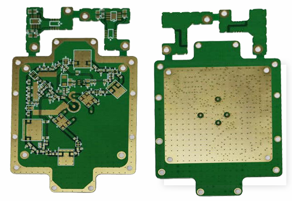
There are as many as 20 processes in the PCB design and production process. Poor soldering is really a headache. Poor tin on the circuit board may cause such as circuit sand holes, wire breakage, circuit dog teeth, open circuits, and circuit sand holes. ; If the hole copper is too thin, the hole will be formed without copper; if the hole copper is too thin, the hole will be formed without copper. If the hole is too thin, the hole will be formed without copper; Problems, so encountering poor soldering often means re-soldering or even abandonment of previous efforts and re-production. Therefore, in the PCB industry, it is very important to understand the reasons for poor soldering.
The appearance of poor soldering is generally related to the cleanliness of the empty PCB surface. If there is no pollution, there will be basically no poor soldering. Second, poor flux and temperature during soldering. Then the common electrical tin defects of printed circuit boards are mainly reflected in the following points:
1. There are particulate impurities in the plating layer on the board, or grinding particles are left on the surface of the circuit during the manufacturing process of the substrate.

2. There are grease, impurities and other sundries on the board surface, or there are residual silicone oil
3. There are flakes on the surface of the board without tin, and there are particulate impurities in the plating layer on the board.
4. The high-potential coating is rough, there is a burning phenomenon, and there are flakes on the surface of the plate without tin.
5. The tin surface of the substrate or part is seriously oxidized and the copper surface is dull.
6. The plating on one side is intact, and the plating on the other is poor, and there is obvious bright edge phenomenon on the edge of the low-potential hole.
7. There are obvious bright edges on the edges of low-potential holes, and the high-potential coating is rough and burnt.
8. There is no guarantee of sufficient temperature or time during the soldering process, or the flux is not used correctly
9. Tin can not be plated on a large area at low potential, and the surface of the board is slightly dark red or red, with a complete coating on one side, and a poor coating on the other side.
The reasons for the poor electrical tin of the circuit board are mainly reflected in the following points:
1. The composition of the bath liquid is out of balance, the current density is too small, and the plating time is too short.
2. The anodes are too few and unevenly distributed.
3. The tinting agent is out of balance in a small amount or an excessive amount.
4. The anode is too long, the current density is too large, the local wire density of the pattern is too thin, and the light agent is out of adjustment.
5. There is residual film or organic matter locally before plating.
6. The current density is too large, and the plating solution is not sufficiently filtered.
The following summarizes the improvement and prevention plan of PCB board electro-tin defects:
1. Regular chemical analysis and analysis of the ingredients of the syrup are added in time to increase the current density and prolong the plating time.
2. Check anode consumption from time to time and add anodes reasonably.
3. Hearst cell analysis adjusts the content of the light agent.
4. Reasonably adjust the distribution of anodes, reduce the current density by an appropriate amount, reasonably design the wiring or jointing of the board, and adjust the light agent.
5. Strengthen the pre-plating treatment.
6. Reduce the current density, and regularly maintain the filter system or perform weak electrolysis treatment.
7. Strictly control the storage time and environmental conditions of the storage process, and strictly operate the production process.
8. Use a solvent to clean the sundries, if it is silicone oil, then you need to use a special cleaning solvent to wash
9. Control the temperature in the PCB soldering process at 55-80 degree Celsius and ensure sufficient preheating time
10. Use soldering flux correctly.
The above is the relevant knowledge about the poor tin in PCB design.