A, PCB simulation and DDR3 memory design
1 Overview Today's computer system DDR3 memory technology has been widely used, and the data transmission rate has been repeatedly promoted, and now it is as high as 1866Mbps.
Under the condition of this kind of high-speed bus, in order to ensure the reliability of data transmission quality and meet the timing requirements of the parallel bus, it poses a great challenge to the design and implementation.
This article mainly uses Cadence's time-domain analysis tool to quantitatively analyze the DDR3 design, introduces the main factors that affect the signal integrity of DDR3 timing analysis, and improves and optimizes the design through the analysis of the results to improve the signal quality. Its reliability and safety are greatly improved.
2 Introduction to DDR3 DDR3 memory is similar to DDR2 memory, including 2 controllers and memory parts, all of which use source synchronous timing, that is, the selected signal (clock) is not sent by a separate clock source, but by the driver chip.
It has a higher data transfer rate than DR2, up to 1866MBPS; DDR3 also uses 8-bit prefetch technology, which significantly increases the storage bandwidth, and its operating voltage is 1.5V, ensuring reduced power consumption at the same frequency. DDR3 interface design is difficult to achieve. It uses a unique Fly-by topology and uses "write equalization" technology to control the internal offset timing of the device and other effective measures.

Although it plays a role in ensuring design implementation and signal integrity, the storage system that achieves high frequency and bandwidth is not comprehensive. Therefore, simulation analysis is necessary to ensure the integrity of design implementation and signal quality.
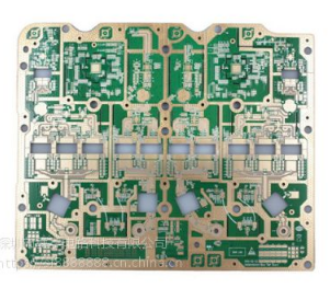
3 Simulation analysis DDR3 simulation analysis combined with the project to explain: choose PowerPC 64-bit dual-core CPU module, this module uses Micron's MT41J256M16HA-125IT for memory.
Analyzing the processor of P5020, the module is configured with a memory bus data transmission rate of 1333MT/s and an analog frequency of 666MHz.
3.1 Pre-simulation preparation Before the analysis, it is necessary to communicate with the PCB manufacturer based on the impedance of DDR3 to confirm its laminated structure. The key to ensuring the performance of the transmission line in high-speed transmission is the continuous characteristic impedance. Determine the impedance control of the high-speed PCB signal line within a certain range, so that the printed circuit board becomes a "controllable impedance board", which is the basis of analog analysis.
The single line impedance of the DDR3 bus is 50Ω, and the differential linear impedance is 100Ω. Set the voltage value of the analysis network terminal, including the passive device allocation model of the analyzed device, determine the device type attributes, and ensure the device pin attributes (input and output, power grounding, etc.)......
Second, quickly solve the signal integrity in the PCB high-speed system
Quickly solve signal integrity problems in PCB high-speed systems. With the increase of data rates, signal integrity problems have become the most critical factor considered by design engineers. This exponential increase in data rates can be seen in applications such as high-bandwidth routers/switches such as handheld mobile devices and consumer display products. Jitter (noise) is the main reason for reducing the level of signal integrity in the design. In addition to using layout, impedance matching and more expensive materials to achieve signal integrity enhancement technology, designers can also simply add jitter receivers such as equalizers to the design to solve the jitter problem.
In this way, designers do not have to focus on signal integrity issues, but on the core design of the system. Signal wiring was often regarded as a simple concept in the past, and there is no distinction between video signals, voice signals, or data signals from the point of view of the wiring. Therefore, few people cared about signal wiring in the past. However, now the situation has completely changed. The video signal transmission speed has now reached 3.3Gbps per channel, and the data signal far exceeds 5Gbps per channel.
High-speed serial standards such as PCI Express, XAUI, SATA, TMDS, and Display Port require design teams and engineers not only to consider signal integrity issues, but also to have an in-depth understanding of how it will affect system performance and reliability. . In order to master this knowledge, engineers must first understand the factors that affect signal integrity in the system. The loss of signal integrity in the system can be observed by increasing the signal jitter. The total jitter of the system is mainly composed of two kinds of jitter, namely random jitter and deterministic jitter. Random jitter is infinite and basically obeys Gaussian distribution, while deterministic jitter is finite and predictable.
In 90% of systems, deterministic jitter is the main signal integrity problem that design engineers must solve. Deterministic jitter includes code interference (ISI), duty cycle distortion, and periodic jitter, which are caused by bandwidth limitation issues, clock cycle asymmetry, and cross-coupling or EMI issues, respectively.
Passive components such as connectors, PCB wiring, long cables and other passive components placed along the wiring are the most important sources of deterministic jitter. The higher the signal frequency, the greater the attenuation, so the power level in the specified data stream does not match, and this power level mismatch will result in ISI in the signal.
ISI will reduce signal integrity, which is enough to prevent the receiver from correctly extracting any actual data from the signal at the receiving end. The reason for the power level mismatch is that no design engineer can guarantee the data transmission in the design. The data can be constantly changing (0-1-0-1-0-1, etc.) or constant (1-1-1-1-1-1, etc.). Obviously, the duty-free ratio of the above 6 changing bits is 6 times the duty ratio of the 6"1" constant data stream. Since the duty-free ratio is 6 times smaller, the signal frequency will be 6 times higher.
If the data stream contains these two types, the receiver signal will have very different power levels, because the higher the frequency, the greater the attenuation.
Solve the problem of power mismatch Most high-speed signal standards stipulate that the number of continuous bits without change should be minimized, such as 8B/10B encoding. This coding scheme ensures that the data stream does not exceed 4 consecutive bits.
However, it is still possible to quadruple the high power portion of the receiver signal. To compensate for the power level mismatch to reduce ISI, PCB designers can use equalization or de-emphasis techniques.
The PCB equalization technology will increase the power of all high-speed bits, so that the received signals in the high-speed and low-speed bits have the same power level, thereby reducing power level mismatch. The opposite of exacerbating balance, but the goal is the same: minimizing power level mismatch. It is done by reducing the power of the low-speed bit, which will increase the power of the high-speed bit.