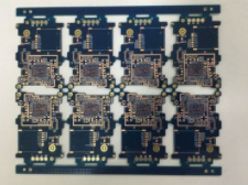
Common need manual placement of a variety of table stick transformers, connectors, TO package integrated circuits, etc. These devices are still subject to assembly errors. General repair is carried out manually, this link is also prone to welding reverse problems. Therefore, it is necessary to explain the corresponding relationship between the positioning method of components and the pad and screen printing of components on the PCB board.
1. Capacitance
For the aluminum through hole as shown in the following figure, the electrolytic capacitor is generally expressed by the length of the foot and the mark on the body. Long feet are positive, short feet are negative. There are also white or other stripes parallel to the pins on the negative side of the housing.

One way is to put a "+" sign directly on the positive side. The advantage of this method is that it is convenient to check polarity after welding. Disadvantage is to occupy a larger area of the circuit board. The second method is to use silk screen to fill in the area where the negative pole is located. This polarity representation occupies a small area of the circuit board, but it is not convenient to check the polarity after welding. It is common in the occasions where the density of circuit board components such as computer motherboards is large. The marking method of the capacitor on the circuit board can refer to the aluminum electrolytic capacitor. For surface attached aluminum electrolytic capacitor, ink coated side is negative, positive side base is generally processed by Angle cutting.
2. Diode
For light-emitting diodes, the general use of the length of the foot to express the positive and negative, the long foot is positive, short foot is negative. Sometimes they cut off a little bit on the side of the LEDS, and this can also be used to indicate the negative electrode. On the circuit board, silk screen printing "+" is generally used to indicate the positive pole. The polarity of the diode is indicated by the screen print on the circuit board. This is more graphic. The other is to draw the schematic symbol of the diode directly on the silk screen circuit board. The polarity representation of surface led is very confusing. Sometimes there are different representations between different package types within a manufacturer. But the common color point or color bar is painted on the cathode side of the LIGHT-emitting diode, and there are also corners cut on the cathode side.
3. Integrated circuits
For DIP and SO package integrated circuits with pins distributed on both sides, the upper half circle notch is generally used to indicate that this direction is the top of the chip, and the upper left first pin is the first pin of the chip. Also useful screen printing or laser in the top to play a line to express. In addition, there are directly in the chip first foot next to the body with silk screen dot or directly in the injection molding press a pit. Some integrated circuits are also represented by cutting a hypotenuse across the body of the starting edge of the first leg. For quad package QFP, PLCC, BGA:QFP integrated circuit generally uses concave dot, silk screen dot, or according to the type of silk screen to judge the direction on the body corresponding to the first pin. Some use the method of cutting off an Angle to represent the first foot, then the counterclockwise direction is the first foot. Note that sometimes there are 3 pits on a chip, so the corner without pits corresponds to the lower right side of the chip.
4. Other devices
The plugins on the object are generally controlled by positioning the gap. Some write a 1 near the first foot or use a triangle to represent the first foot. Other devices generally draw silk screen on the circuit board consistent with the real object to avoid wrong insertion. For through-hole installation of resistance, generally in the circuit board with silk screen to circle the common end of the way, or write 1 near the first foot. In order to regulate the requirements of pads, screen printing and blocking welding of components on the circuit board, IPC has issued two related standards, namely, IPC-7351 and IPC-SM-840. However, in actual use, the device direction marking symbols made by the device direction representation method defined by IPC are often shielded by the device body after welding, which is not suitable for inspection. Therefore, the graphic design of the pad of components should be adjusted according to the actual situation.
In a word, in physical objects, discrete devices generally adopt the method of long and short pins and screen printing or coloring to express polarity. For integrated circuits, concave, screen printing, notch, missing Angle, missing edge or direct indication are often used to mark the first leg. In the production of pad graphics, generally should be as far as possible according to the device shape drawing, and as much as possible to the device shape and positioning information reflected through the form of screen printing, in order to avoid manual assembly, welding errors.