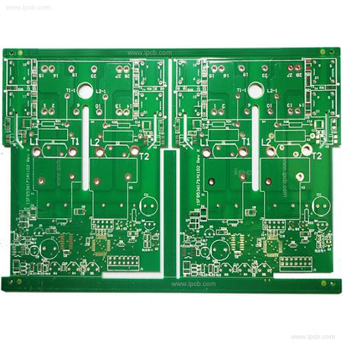
1. PCB Ceramic substrate manufacturing technology
There are many types of ceramic products manufacturing technologies in PCB factories. It is said that there are more than 30 manufacturing processes, such as dry pressing, slurry, extrusion, injection, seeding and isostatic pressing, because electronic ceramic substrates are "flat" Type (block or round), the shape is not complicated, and the dry molding and processing are used. For example, the manufacturing process is simple and the cost is low. Therefore, most of the dry molding methods are used. The manufacturing process of dry-pressed flat electronic ceramics mainly includes three aspects, namely the formation of the blank, the sintering and finishing of the blank, and the formation of a circuit on the substrate.
1. Green symbiosis manufacturing (forming)
Use high-purity alumina (95% Al2O3) powder (depending on the use and manufacturing method, different particle sizes are required). For example, from a few illiterate to tens of microns) and additives (mainly binders, dispersants, etc.) to form "slurry" or processing materials.

1: The dry pressing method produces a green body (or "green body").
The dry compaction is made of high-purity alumina (alumina content used for electronic ceramics is greater than 92%, most of which is 99%) powder (for dry compaction, the particle size should not exceed 60 m, and for extrusion, elongation, and use) Appropriate plasticizers and binders control the particle size of powders within 1 m). After the dry pressed billets are uniformly mixed, the offspring of the pieces or fish fillets can now reach 0.50 mm, or even 0.3 mm (related to the plate the size of). The dry-pressed blank can be processed before sintering, such as shape size and drilling, but pay attention to the size compensation caused by sintering (expanding the size of the disc pattern).
2: The green body is manufactured by the casting method.
Liquid (aluminum oxide powder, solvents, dispersants, adhesives, adhesives, plasticizers, etc. are uniformly mixed and passed through a sieve) manufacturing, expansion flow (the glue is evenly coated on the metal or heat-resistant polyester tape on the expansion machine), Drying, trimming (also can be processed into holes, etc.), skimand, skimand sintering and other processes. Production can be automated and expand the scale of PCB production.
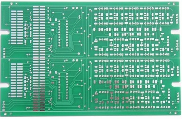
Two, PCB design schematic drawing skills
When designing a drawing on the PCB, ERC will display a "Multiple Net Identifiers" error message:
Solution: It may be because different network labels are connected together during PCB design, or the same connection gives different network labels.
If it is a single schematic diagram, you can find the position with the wrong label on the schematic diagram. When you use multiple schematic diagrams, especially when editing multiple layers, all schematic diagrams may be found in sub-diagrams.
1: Common errors in PCB schematics:
ERC reports that there is no access signal for this pin.
A sort of. When the package is created, I/O attributes will be defined for the pins. For example, linking input and output ports together can cause errors. In fact, if there is no protel for circuit simulation, there is no need to define the I/O properties of the pins.
When building or placing components, inconsistent grid properties are modified, and the pins are not connected to the wires.
When assembling the component, the pin direction is opposite, and it must not be connected at the pin name end.
2: ERC reports duplicate network tags (error: multiple network identifiers).
This may be because different network labels are connected together, or different network labels are given on the same connection. It is important to note that the error indicated by PROTEL is not necessarily an actual error, or may be wrong on other schematics (if there is a layered circuit diagram)
3: The component runs outside the graphic boundary: no component is created in the center of the component library chart paper.
4: The created project file netlist can only be partially adjusted to PCB: the netlist is generated without selecting the global.
5: When using your own multi-part creation components, do not use comments.