As one of the most important components in the contemporary electronic component industry, PCB boards are applied to almost all electronic products and are called "the mother of electronic system products". With the ever-increasing requirements of PCB quality, in order to better realize the quality information management and control of products in production, information traceability systems such as marking characters, bar codes, and two-dimensional codes on PCB boards have emerged.
At present, PCB marking processing mainly includes two methods: silk screen printing and laser marking.
Traditional silk-screen printing uses a well-made graphic screen, and uses external pressure to make the character ink penetrate through part of the mesh of the screen and miss the printing on the surface of the circuit board. The remaining part of the mesh on the screen will be blocked and will not penetrate the ink. Only a blank will be formed on the surface of the circuit board. The missing ink will form characters, logos, patterns, etc. This processing method is relatively cheap and fast, but it has the disadvantages of rough marking effect, easy to fall off the marking, inability to mark small PCB boards, and chemical raw materials that have certain toxicity.

Laser marking uses high-energy-density lasers to locally irradiate the PCB board to vaporize or discolor the surface material, thereby leaving a permanent mark. This non-contact processing can mark a very clear two-dimensional code on a very small format, ensuring high precision and high quality, and will not be worn due to high and low temperature, acid-base changes and external friction. No chemical substances are required, and there is no negative effect on personnel safety and the environment.
The use of PCB special laser marking machine, with its precision and flexibility, can make up for the shortcomings of screen printing, greatly improve production efficiency and yield, reduce costs, and reduce pollution. Laser marking is gradually becoming the best method for PCB marking, and has been widely used in many fields such as digital products, wearable devices, and automotive circuit boards.
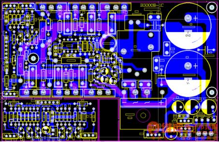
Have you mastered the methods and skills of PCB recognition?
As the PCB drawing is relatively "chaotic", the following methods and techniques can be used to improve the speed of image recognition.
1. According to the appearance characteristics of some components, these components can be easily found, such as integrated circuits, power amplifier tubes, switches, and transformers.
2. For integrated circuits, a specific integrated circuit can be found according to the type on the integrated circuit.
There are no rules for the distribution and arrangement of PCB components, but the components in the same unit circuit are relatively concentrated.
3. Some unit circuits have characteristics, and they can be easily found based on these characteristics. For example, there are more diodes in the rectifier circuit and a heat sink on the power amplifier tube. The filter capacitor has the largest capacity and largest volume.
4. When looking for the ground wire, the large area copper foil circuit on the circuit board is the ground wire, and the ground wire on a circuit board is connected everywhere.
In addition, the metal shell of some components is grounded. When looking for a ground wire, any of the above can be used as a ground wire. In some machines, the ground wires are also connected between the circuit boards, but when the connectors between each circuit board are not connected, the ground wires between the circuit boards are blocked. One point should be paid attention to when overhauling.
5. In the process of comparing the PCB diagram with the actual circuit board, draw the same recognition direction on the PCB diagram and the circuit board respectively, so that the PCB diagram can have the same recognition direction as the circuit board, saving every It is necessary to compare the direction of recognizing the picture every time, which can greatly facilitate the recognizing of the picture.
6. When observing the connection between the components and the copper foil circuit on the circuit board and observing the direction of the copper foil circuit, you can use a lamp to shine. Place the lamp on the side with the copper foil circuit, and the connection between the copper foil circuit and the components can be clearly and conveniently observed on the side with the components, so there is no need to flip the PCB circuit board. Constantly flipping the PCB circuit board is not only troublesome, but also easy to break the leads on the circuit board.