In the research of PCB reverse technology, the reverse schematic diagram refers to the PCB circuit diagram based on the PCB file diagram or directly based on the physical description of the product to illustrate the principle and working conditions of the PCB board. In addition, the circuit diagram is also used to analyze the functional characteristics of the product itself.
In forward design, general product research and development should first carry out schematic design, and then carry out PCB design according to the schematic. Whether it is used to analyze the principle of the circuit board and the reverse research of the working characteristics of the product, or as the basis and basis of the PCB design in the forward design, the PCB schematic diagram has a special role.
Then, how to reverse the PCB schematic diagram according to the document or object, and what details should be paid attention to during the reverse calculation?

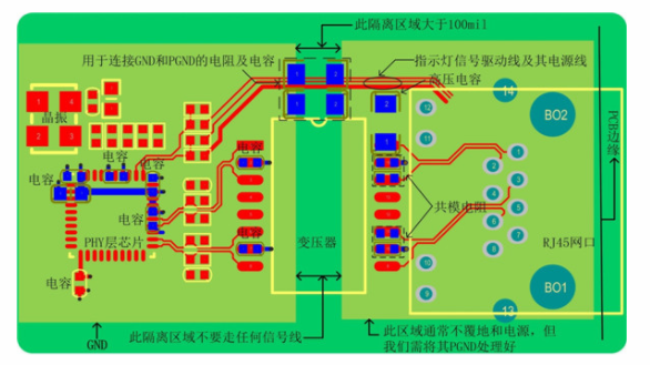
1. Reasonable division of functional areas In the reverse design of a good PCB circuit board schematic diagram, proper division of functional areas can help engineers reduce unnecessary troubles and improve drawing efficiency.
Under normal circumstances, the components on the PCB have the same functions, and the centers are arranged, and the functional areas can be conveniently and accurately based on the reverse schematic diagram. However, the division of the functional area is not random. It requires engineers to have a certain understanding of the relevant knowledge of electronic circuits. First, find out the core components in the functional unit, and then according to the wiring connection, you can find other components of the same functional unit to form functional partitions. The formation of functional zones is the basis of the diagram.
In addition, during this process, don't forget to cleverly use the component numbers on the PCB circuit board, which can help you partition functions faster.
Second, find suitable reference parts
This data can also be said to be in the schematic diagram of the main components of the PCB circuit board network city at the beginning of use. After the data is determined, it is drawn based on the pins of these reference components to ensure the accuracy of the schematic diagram to a greater extent.
For engineers, the determination of reference parts is not very complicated. Generally speaking, you can choose to play a major role in circuit components as a reference. They are generally relatively large, with many pins, and easy to draw, such as integrated circuits. Transformers, transistors, etc., can be used as suitable reference components.
Third, correctly distinguish the lines, reasonable drawing and wiring. For the distinction between ground wires, power wires, and signal wires, engineers also need to have relevant power supply knowledge, circuit connection knowledge, PCB wiring knowledge, etc.
The difference between these lines can be analyzed in terms of component connection, the width of the wire copper foil and the characteristics of the electronic product itself.
In the wiring diagram, in order to avoid the crossing and interpenetration of wires, a large number of grounding symbols can be used for the ground wire. Various lines can use different lines of different colors to ensure clearness and legibility. Various components can also use special signs, or even The unit circuits can be drawn individually and finally combined.
Fourth, master the basic framework and learn the same schematics
For some basic electronic circuit frame composition and principle drawing methods, engineers need to master, not only to be able to directly draw some simple and classic unit circuit basic composition forms, but also to form the overall frame of the electronic circuit.
On the other hand, don't ignore that the same type of electronic products have certain similarities in schematic diagrams. In PCB network cities, engineers can learn from similar circuit diagrams based on their experience and develop new product schematic diagrams.
V. After adjusting and optimizing the schematic diagram, the test and inspection link must be passed, indicating that the reverse design of the PCB schematic diagram has ended.
It is necessary to check and optimize the nominal values of components that are sensitive to PCB distribution parameters. According to the PCB document diagram, compare, analyze and check the schematic diagram to ensure that the schematic diagram is exactly the same as the document diagram. If the layout of the schematic diagram is found to be inconsistent with the requirements in the inspection, the schematic diagram will also be adjusted until it is completely reasonable, standardized, accurate and clear.