Through the analysis and discussion of existing product technical documents, design ideas, structural features, process technology, etc., it can provide feasibility analysis and competitive reference for the development and design of new products, and assist R&D and design units to follow up the latest technological development in time Trends, timely adjustment and improvement of product design plans, and research and development of the most competitive new products in the market.
The process of PCB copying can realize the rapid update, upgrade and secondary development of various types of electronic products through the extraction and partial modification of technical data files. Willing to optimize the design and change the PCB.
It is also possible to add new functions to the product or redesign the functional features on this basis, so that products with new functions will be unveiled at the fastest speed and with a new attitude, not only having their own intellectual property rights, but also in the market It has won the first opportunity and brought double benefits to customers.
Whether it is used to analyze circuit board principles and product operating characteristics in reverse research, or is reused as the basis and basis of PCB design in forward design, PCB schematics have a special role.

Attention to detail
1. Reasonably divide functional areas
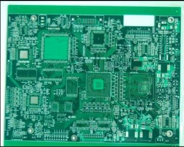
When performing the reverse design of the schematic diagram of a good PCB circuit board, a reasonable division of functional areas can help engineers reduce some unnecessary troubles and improve the efficiency of drawing.
Generally speaking, components with the same function on a PCB board are arranged in a concentrated manner, and the division of areas by function can have a convenient and accurate basis when inverting the schematic diagram.
However, the division of this functional area is not arbitrary. It requires engineers to have a certain understanding of electronic circuit related knowledge.
First, find the core component in a certain functional unit, and then according to the wiring connection, you can find other components of the same functional unit along the way to form a functional partition.
The formation of functional partitions is the basis of schematic drawing. In addition, in this process, don't forget to use the component serial numbers on the circuit board cleverly. They can help you partition the functions faster.
2. Find the right reference parts
This reference part can also be said to be the main component PCB net city used at the beginning of the schematic drawing. After the reference part is determined, it is drawn according to the pins of these reference parts, which can ensure the accuracy of the schematic drawing to a greater extent. sex.
For engineers, the determination of reference parts is not very complicated. Under normal circumstances, the components that play a major role in the circuit can be selected as reference parts. They are generally larger in size and have more pins, which is convenient for drawing. Such as integrated circuits, transformers, transistors, etc., can all be used as suitable reference components.
3. Correctly distinguish lines and draw wiring reasonably
For the distinction between ground wires, power wires, and signal wires, engineers also need to have relevant power supply knowledge, circuit connection knowledge, PCB wiring knowledge, and so on. The distinction of these lines can be analyzed in terms of the connection of components, the width of the copper foil of the line, and the characteristics of the electronic product itself.
In the wiring drawing, in order to avoid the crossing and interpenetration of lines, a large number of grounding symbols can be used for the grounding line. Various lines can use different lines of different colors to ensure that they are clear and identifiable. For various components, special signs can be used, or even Draw the unit circuits separately, and finally combine them.
4. Master the basic framework and learn from similar schematic diagrams
For some basic electronic circuit frame composition and principle drawing methods, engineers need to be proficient, not only to be able to directly draw some simple and classic unit circuits, but also to form the overall frame of electronic circuits.
On the other hand, don't ignore that the same type of electronic products have a certain similarity in the schematic diagrams. Engineers can use the accumulation of experience and fully learn from similar circuit diagrams to reverse the schematic diagrams of new products.
5. Check and optimize
After the schematic drawing is completed, the reverse design of the PCB schematic can be said to be completed after testing and verification. The nominal value of the components sensitive to the PCB distribution parameters needs to be checked and optimized. According to the PCB file diagram, the schematic diagram is compared and analyzed to ensure that the schematic diagram is completely consistent with the file diagram.