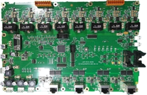
1. Lead metal whose work is in welding
The low-temperature soft soldering of PCB circuit boards has always been based on eutectic (or eutectic) tin-lead alloy (S n 6 3 / Pb 37). Not only is the quality good, easy to operate, and reliable, but also the technology is mature, the supply is intact, and the price is low, all of which can be attributed to the participation of lead. Its only fatal disadvantage is that it is toxic and harmful to the human body. Nowadays, lead must be removed when environmental protection is in charge. Not only is the performance of all kinds of lead-free solders far inferior to those with lead, but there is no substitute for it. When I was about to leave forever, I suddenly thought of [Lead], where is the sacred? And how can it be so outstanding? The following is a summary of some of the important functions of lead in soldering for you to understand :
This is a homogeneous structure of tin-lead alloys in various proportions
A. Lead can be easily melted with tin in any ratio to form a homogeneous alloy. There will be no incompatible D en dr ite SIMC between each other. At most, it is only divided into lead rich area (Lead Rich area), which is a single color area after microetching. The lead content is between 50-70%wt), or the tin rich area (the tin rich area is black after microetching, and the tin content is 5 to 80%wt). Lead is the only metal that can work closely with tin.

B. Lead is 11 times cheaper than tin, which can reduce the cost of solder. In addition, when lead is present, the rate of dissolving the solid Cu into the liquid S n will be slowed down, which can reduce the appearance of branched dumb IMC in the solder joint, and improve the soldering strength in a very homogeneous state.
C. The melting point of lead is 32 2 degree Celsius, and the melting point of tin is 2 3 1 degree Celsius. After alloying, the melting point decreases. The eutectic composition is S n 6 3 /P b 37 m. p. Only 183 degree Celsius, no harm to electronic parts and circuit boards.
D. Tin whiskers will no longer grow after adding lead to more than 20%, and the various formulas of tin-lead electroplating are very mature, which is very convenient for parts feet and PCB electroplating. Of course, the tin-lead film or solder joints will not grow long.
E. The lead-tin alloy S n 6 3 has a low surface tension (380 dyn e/260 degree Celsius, which means less cohesion), low heat consumption, easy to touch tin, very short dip time (average 0.7 seconds), contact angle Very small. As for the lead-free SAC305, which is most promising to become the mainstream, its surface tension is as high as 460 dyne/260°C, the tin-dipping time is as long as 1.2 seconds, and the contact angle is 4 3-4 4°. The solder pads often expose copper when it is not easy to loose tin.
F. The lead-tin alloy is very soft, and the structure is fine and uniform after solidification, and it is not easy to crack. SAC305 has a hard texture after curing (B a 1l S h e ar Te S t’s false high reading value, which often causes lead-free is better than lead-free misleading, and the heterogeneous structure is rough and easy to crack.
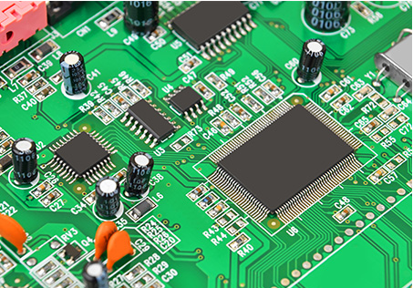
2. IMC of tin-silver-copper lead-free solder processed by SMT
In terms of SAC305 (3.0% Ag, 0.5% Cu and the rest are S n, SAC305 for short), it is very difficult to achieve uniform distribution of the components during its preparation. Therefore, it is almost impossible to achieve an overall homogeneous eutectic composition. possible. It is impossible to reach the homogeneity state of Sn63/Pb37 during the heating and cooling process without passing through any Pasty State, but directly back and forth between liquefaction and solidification, and its structure can almost reach the homogeneous state without obvious dendrites.
During SAC305 cooling, some parts of pure tin will first solidify at the beginning, and it will be dispersed to form a branch-like frame. When other remaining liquid materials continue to cool and solidify in each empty frame, they will shrink and shrink in volume, and then form Slightly cracked constriction (the central part of the outer surface where a piece of solder finally cools). Once vibration occurs during transportation, various microcracks may expand, resulting in poor strength. Unless the SAC305 can be welded with a rapid cooling rate (for example, 5-6°C/SeC), the overall structure will become more delicate under the condition of reducing the appearance of branches and being more homogeneous.
It is difficult for the non-homogeneous solder alloys to achieve the ideal state of eutectic in PCB lead-free soldering
Heterogeneous solder alloys are difficult to achieve, the ideal state of eutectic, so a "pasty" (pasty) will appear during the solidification process, that is, a solid phase (Dendrite) and a liquid phase will coexist temporarily The transitional period. Until the entire solidification is completed, there will be more impurities and fragile and unstable borders.
Micro-cracking phenomenon in circuit board welding
The melting point of tin is 231°C, silver is 961°C, copper is 1083°C, and the mp of SAC305 is only 217°C. Therefore, it is known that the addition of 3% silver and 0.5% copper has reached the effect of lowering the melting point of the alloy. The addition of Ag can also increase the hardness and strength of the solder joint, but it will also quickly form a long IMC of Ag3S n in the solder joint, which will have an adverse effect on the long-term reliability. After adding copper, there is another benefit of reducing the infiltration of extra copper. In lead-free solder for wave soldering, once the amount of copper exceeds 1.0% by weight, needle-like crystals will often appear inside and on the surface of the solder joint. Not only the strength is reduced, but also the trouble of short circuit when the needle body is too long.
Wave soldering PCB processing, whether it is SAC or tin-copper alloy (99.3Sn, 0.7Cu), is prone to excessive copper contamination. The general way to solve the problem is to add tin or tin and silver instead of copper when supplementing. However, how to improve the management process still requires a lot of practical experience.
When the copper contamination of lead wave soldering is too high, the uneven surface to be soldered will have an adverse effect on the strength of the solder joints.
In lead-free wave soldering, excessive copper pollution often causes problems of bridges and icebergs