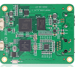
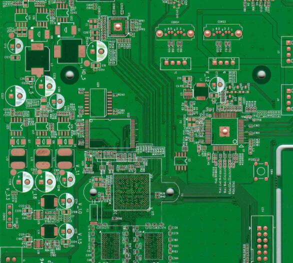
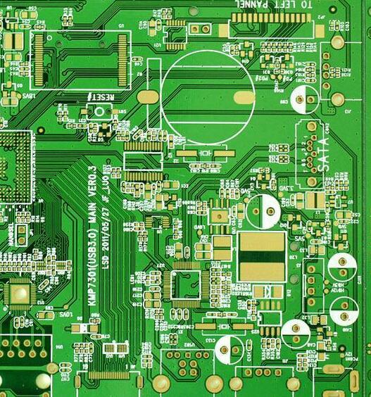
With the rapid development of electronic technology, miniaturization, miniaturization, BGA, and high-density chip spacing are becoming more and more common, and the requirements for PCB soldering technology are getting higher and higher.
In PCB processing plants, false soldering has always been the worst, and false soldering can lead to unstable product performance. What is particularly troublesome is that, like other bad soldering, virtual soldering cannot even be found in the subsequent ICT and FT tests, leading to the flow of problematic products to the market and even a huge loss of brand and reputation.
For the virtual welding of smT patch and DIP plug-in welding, the reasons for this analysis are as follows:
1: Virtual welding caused by poor welding of components (including poor welding of functional modules)
2: Virtual soldering caused by poor PCB soldering.
3: Due to the universality of virtual welding.
4: Empty soldering caused by insufficient solder paste performance (including solder paste quality)
5: Virtual welding is caused by improper process control.

Definition of false welding:
Weak soldering refers to the lack of tin on the pins, soldering ends, and PCB pads of the components. The wetting angle of the solder here is greater than 90 degrees, and only a small amount of solder wets the pins, soldering ends, and PCB pads, resulting in poor contact. And intermittently.
Virtual soldering refers to the component pins. The solder ends of the tin on the tin are good, and a good solder joint has been formed from the surface, while the solder joint between the internal solder and the PCB pad has not formed a good soldering. When the solder joint is caused by external force Can be easily separated from the mat.
These two defects are common in single-sided copper PCB soldering processes.
Learn more about the reasons for false welding of molybdenum alloys:
1: Oxidation or pollution of the soldering ends, pins, and PCB pads of the components, resulting in poor solderability;
2: The position of the solder joint is contaminated with impurities such as oxides, making it difficult to tin plate.
3: The adhesion of the metal electrode at the welding end of the component is poor, or the cover peeling occurs when a single-layer electrode is used at the welding temperature;
4: The heat capacity of the parts/welding pads is large, and the parts pins and pads have not reached the welding temperature;
5: Improper selection of flux, poor activity or failure, resulting in poor solder joint wettability;
Judgment of virtual welding.
1: Manual visual inspection (including magnifying glass, microscope). When the solder is visually found, the solder immersion is too low, the solder immersion is poor, or the weld is cracked in the middle of the weld, or the surface of the solder is convex, or the solder is not compatible with SMD, etc., all need to be noted, even if it is Minor phenomena can also cause hidden dangers. It should be immediately determined whether there is a batch of virtual welding problems. The judgment method is: check whether there are solder joint problems on more PCBs in the same position, such as only a few PCB problems, which may be caused by solder paste scratches, pin deformations, etc., for example, there are problems in many PCBs in the same position. At this time, it is likely to be caused by bad components or pad problems.
2: Import AOI automatic optical detector instead of manual automatic detection.
3: Causes and solutions of virtual welding.
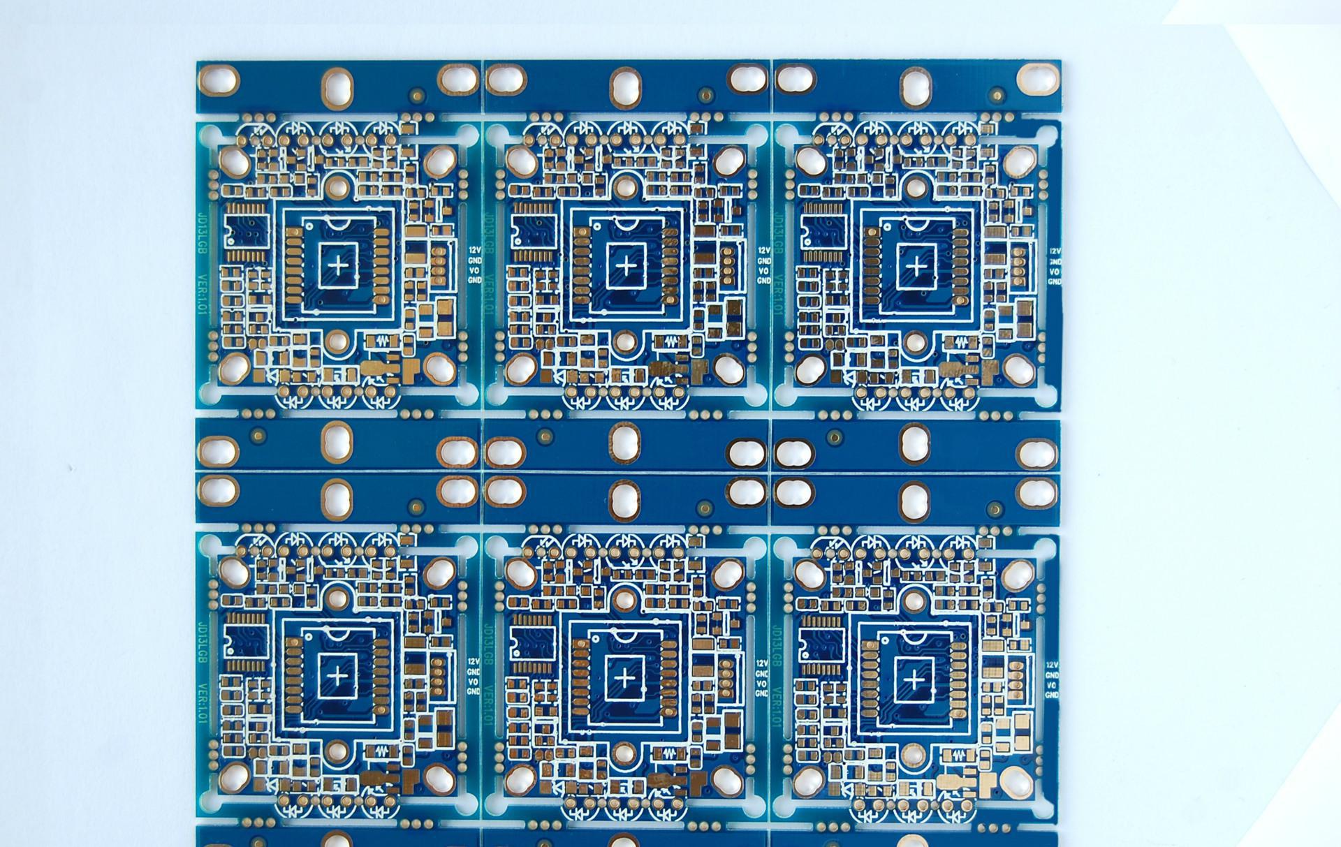
1: The gasket design is defective. There should be no through holes on the pads. The through holes will cause solder loss due to insufficient solder. The pad spacing and area also need to be matched with standards, otherwise the design should be corrected as soon as possible.
2. The PCB board is oxidized, that is, the pad is not bright. If oxidation occurs, an eraser can be used to erase the oxide layer in order to reproduce its bright light. The PCB board is susceptible to moisture. If in doubt, it can be dried in a drying oven. The PCB board is polluted by oil stains, sweat stains, etc. At this time, it should be cleaned with absolute ethanol.
3: On the PCB printed with solder paste, scrape and scrape the solder paste to reduce the amount of solder paste on the relevant pads, thereby making the solder paste insufficient. It should be added in time. The filling method can be used in the batching machine, or it can be supplemented by picking a little bit with a bamboo stick.
4: SMD (surface paste composition) is of poor quality, expired, oxidized, deformed, and caused false welding. This is the more common cause.
1: The oxidized component does not emit light. The melting point of the oxide increases. At this time, you can use electric ferrochrome and loose flux above 300 degrees for welding, but when using SMT above 200 degrees for ring welding, you should use less corrosive no-clean flux. The solder paste is difficult to melt. . Therefore, reflow ovens should not be used to solder oxidized SMDs. When purchasing components, please make sure to check for oxidation and repurchase them for use in time. Similarly, solder oxide paste cannot be used.
2: Surface-mounted components with multiple legs. The legs are very small and easily deformed under the action of external force. Once deformed, there will definitely be virtual welding or lack of welding. Therefore, it is necessary to carefully check and repair in time before welding.
3: For PCBs printed with solder paste, scrape and scrape the solder paste to reduce the amount of solder paste on the relevant pads, which will lead to a shortage of solder paste and should be filled in time.
Precautions for false and false welding:
1: Strict supplier management to ensure stable material quality;
2: Components, PCBs, etc. are on a first-come, first-served basis, strictly moisture-proof to ensure the validity period during the use period;
3: If the PCB is contaminated or expired and oxidized, it needs to be cleaned before use;
4: Clean the oxides at the tin furnace, channels and nozzles to ensure a clean flow of solder;
5: Three-layer end structure welding rod is used to ensure that it can withstand two peak welding temperature shocks above 260°C;
6: For components with large heat capacity and PCB pads, the preheating method has been improved, and a certain amount of heat has been supplemented;
7: Choose a flux with higher activity and ensure that it has been stored and used in accordance with the operating regulations;
8: Set an appropriate preheating temperature to prevent premature aging of the flux.