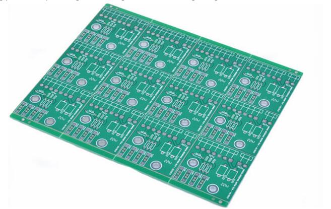
Copper pour is a common operation, which is to cover the area of the circuit board without wiring with copper film. This can enhance the anti-interference performance of the circuit board. The so-called copper pour is to use the unused space on the PCB circuit board as the reference surface, and then fill it with solid copper. These copper areas are also called copper filling. Copper coating can reduce ground wire impedance and improve anti-interference ability; reduce voltage drop and improve power supply efficiency; in addition, connect to ground wire to reduce loop area.
There are several issues to be dealt with in copper coating:
1. Single-point connection of different grounds: The method is to connect through 0 ohm resistors or magnetic beads or inductance.
2. Copper-clad near the crystal oscillator, the crystal oscillator in the circuit is a high-frequency emission source: the method is to coat copper around the crystal oscillator, and then ground the shell of the crystal oscillator separately.

3. Island (dead zone) problem: If you think it is too big, it won't cost much to define a ground via and add it in.
What are the benefits of copper coating?
Improve power efficiency, reduce high-frequency interference, and another is that it looks beautiful!
Is large-area copper pour or grid copper pour better?
Not generalized. why? If the copper is covered with a large area, if the wave soldering is used, the board may be uplifted or even blistered. From this point of view, the heat dissipation of the grid is better. Usually it is a multi-purpose grid with high anti-interference requirements for high-frequency PCBs, and circuits with large currents in low-frequency circuits are commonly used with complete copper.
At the beginning of the wiring, the ground wire should be treated the same. When routing the ground wire, the ground wire should be routed well. You cannot rely on adding via holes to eliminate the ground pins for the connection after the copper pour. This effect is very bad. Of course, if the grid copper is used, these ground connections will affect the appearance. If you are careful, delete it.
The copper filling is intelligent. This operation will actively determine the network properties of the vias and pads in the copper filling area, which is absolutely in line with the safety distance you set. This is different from drawing copper skin, which does not have this function.
Pouring copper has many functions. Pouring copper on the reverse side of the double panel and connecting it to the ground can reduce interference, increase the laying range of the ground wire, reduce low impedance, and so on. Therefore, after the wiring of the PCB board is basically completed, copper is often poured.
Precautions for copper-clad wiring
1. PCB copper clad safety spacing setting:
The safety distance of copper clad is generally twice the safety distance of wiring. But before there is no copper pour, the safety distance of the wiring is set for the wiring, then in the subsequent copper pour process, the safety distance of the copper pour will also default to the safety distance of the wiring. This is not the same as the expected result.
One stupid way is to double the safety distance after laying out the wires, then pour copper, and then change the safety distance back to the safe distance of the wiring after the copper pour is completed, so that the DRC inspection will not report an error. This method is ok, but if you want to change the copper pour again, you have to repeat the above steps, which is slightly troublesome. The best way is to set a rule for the safety distance of the copper pour separately.
Another way is to add rules. In the Clearance of Rule, create a new rule Clearance1 (the name can be customized), and then select Advanced (Query) in the Where the FirstObjectmatches option box, click QueryBuilder, and then the BuildingQueryfromBoard dialog box appears, in the first line of the dialog box in the drop-down menu Select the default item ShowAllLevels, select ObjectKindis from the drop-down menu under ConditionType/Operator, select Ploy from the drop-down menu under ConditionValue on the right, so IsPolygon will be displayed in QueryPreview, click OK to confirm, the next step is not finished, save completely Will prompt an error:
Next, just change IsPolygon to InPolygon in the FullQuery display box, and finally modify the copper safety gap you need in Constraints. Some people say that the priority of the wiring rules is higher than the priority of the copper pour. If the copper pours, it must also comply with the rules of the safety spacing of the wiring. You need to add the copper pour exception to the safety spacing rules of the wiring. The specific method is in FullQuery Note on notInPolygon inside. In fact, this is completely unnecessary, because the priority can be changed. There is an option priority in the lower left corner of the main page of the rule setting, which increases the priority of the copper-clad safety spacing rule to be higher than the wiring safety spacing rule, so that they can interact with each other. Don't interfere anymore.
2. PCB copper-clad line width setting:
When choosing the two modes of Hatched and None, you will notice that there is a place to set TrackWidth. If you choose the default 8mil, and the minimum line width of the network connected to your copper pour is greater than 8mil when setting the line width range, then an error will be reported during DRC, and you did not notice this at the beginning In detail, there are many errors in DRC after each copper pour.