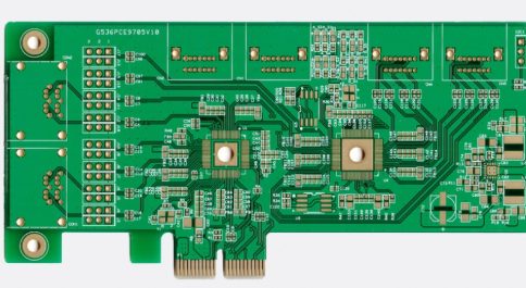
1, Conditioning the whole hole
This word broadly refers to its own "adjustment" or "adjustment" to enable it to adapt to the later situation. In a narrow sense, it means that the dry plates and pore walls are made "hydrophilic" and "positive" before entering the PTH process, and the cleaning work is completed at the same time, so that other subsequent treatments can be continued. Before the PCB through-hole process is launched, the action of arranging the hole walls is called Hole Conditioning.
2, Desmearing
Refers to the PCB board in the high frictional heat of the drilling, when the temperature exceeds the Tg of the resin, the resin will soften or even form a fluid and coat the hole wall with the rotation of the drill bit. After cooling, it will form a fixed paste slag, making the inner layer of copper A barrier is formed between the hole ring and the copper hole wall made later. Therefore, at the beginning of PTH, various methods should be used to remove the scum that has formed, so as to achieve the purpose of subsequent good connection. In the figure, the slag has not been removed, leaving an inconsistent gap between the copper hole wall and the inner hole ring.
3, Dichromate dichromate

Refers to Cr2O7, commonly known as K2Cr2O7, (NH4)2Cr2O7, etc., because there are two chromium atoms in its molecular formula, it is called "heavy" (ㄔㄨㄥ') chromate, in order to interact with chromate (CrO ) Can be distinguished.
4, Etchback Etchback
refers to the multi-layer PCB board on the wall of each through hole, and the resin and fiber glass substrate between the copper ring levels are deliberately etched by about 0.5 to 3 mil, which is called "etch back".
5, Free Radical
When an atom or molecule loses part of its electrons, the charged body formed is called "free radical". Such free radicals have extremely active chemical properties and can be used for special reactions. For example, the "plasma method" for removing slag from the hole wall of a multilayer PCB is the use of free radicals. This method is to put the board in a closed processor with thin air, fill it with O2 and CF4 and apply high voltage to generate various "radicals" and then use it to attack the resin part of the board (not like copper) to reach the hole The effect of internal removal of scum.
6, Negative etch-back
In the early military multi-layer PCB boards or high-grade multi-layer PCB boards, in order to obtain better reliability, apart from cleaning the hole wall glue slag after drilling, it further requires the backing of each dielectric layer to make each inner The layer hole ring can be protruding, so that after the hole wall is plated with copper, a three-bread clip type clamping can be formed. This kind of process that causes the dielectric layer to be eroded and forced to shrink is called "Etch-Back". However, in the general multi-layer PCB board manufacturing process, if the operation is negligent (such as excessive micro-etching or when you want to etch the poor copper hole wall and then redo PTH, the excessive etching that occurs, etc.) will cause the error of the inner copper ring to shrink The phenomenon is called "anti-etch back".
7, Plasma
It refers to certain "non-polymeric" mixed gases. After high-voltage ionization in vacuum, some of the gas molecules or atoms will dissociate and become positive and negative ions or free radicals (Free Radical), and then combine with the original Gases mixed together have high activity and energy, but their properties are quite different from the original gas, so it is sometimes called the "Fourth state of matter". This "fourth state" between the gaseous state and the liquid state can only exist under the continuous supply of strong energy, otherwise it will quickly neutralize and become a low-energy original mixed gas. This kind of "fourth state" is originally expressed in "slurry state". Since it can only exist under high voltage and high electric energy, the Chinese translation is called "plasma".
8, Reverse Etchback
Refers to the through-hole of the multi-layer PCB board, the inner copper ring of the hole is etched abnormally, causing the inner edge of the ring to recede from the surface of the hole wall of the drilled hole, and instead let the base material composed of resin and glass fiber The surface forms a protrusion. In other words, the inner diameter of the copper ring is larger than the hole diameter of the drilled hole, which is called "anti-erosion back". In order to have a more reliable interconnection between the ring of each inner layer of the multi-layer PCB and the copper wall of the PTH, the base material must be set back and the copper ring is deliberately placed on the wall of the hole. It protrudes and forms a three-clip-type solid connection with the copper wall of the hole. This process of shrinking resin and glass fiber is called "Etchback", so the abnormal situation mentioned above is called "Reverse Etchback".
9, Shadowing shadows, eclipse dead corners
The word is often used in the process of removing dross from infrared (IR) welding and through-hole plating in the PCB industry, and the two have completely different meanings. The former means that there are many SMDs on the assembly board, which have been positioned with solder paste at the feet of their parts, and need to absorb the high heat of infrared rays for "fusion welding". During the process, some parts may block the radiation and form shadows., Blocking the transfer of heat, so that it can not fully reach the part of the required place, this situation caused insufficient heat and incomplete welding is called Shadowing. The latter refers to the resin in the dead corners of the upper and lower sides of the inner copper ring during the resin etchback (Etchback) of some high-demand products before the PTH process of the multilayer PCB board, which is often not easily removed by the liquid. Bevel, also known as Shadowing.
10, Swelling Agents; Sweller leavening agent
After drilling the multi-layer PCB board, in order to make it easier to remove the glue residue on the hole wall, the board can be immersed in a high-temperature alkaline bath containing organic solvent to soften the attached glue residue. It is easy to remove.
11, Yield yield, yield, yield
The percentage of good products that pass the quality inspection in the production batch is called Yield.