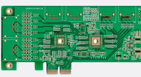
Throughout the entire history of RF multilayer PCB design and processing, the available bonding methods can be roughly divided into the following three categories:
3.1 Direct bonding
In the long history of the manufacture of radio frequency materials and related radio frequency circuit PCB printed boards, the first method of multi-layer realization is direct bonding, or melt bonding.
Direct bonding may have some difficulties in implementation. It is true that this multi-layer bonding method eliminates the need for bonding film materials, but it needs to increase the temperature above the melting point of the dielectric core material to directly fuse the softened PTFE surface together (Figure 1).
Therefore, the choice of direct bonding method must depend on the ability of high-temperature lamination equipment, otherwise, it is just empty talk, and there is no way to talk about implementation.

Of course, some companies face the dilemma of no high-temperature lamination equipment capabilities, and can take the way of laying eggs and cooperating with related PTFE substrate manufacturers to solve the problem of multilayer bonding.
From the perspective of obtaining effective and high-reliability bonding, the direct bonding technology is indeed unique. According to the analysis of professional knowledge (based on the principle of similar compatibility), the bulk bonding is the most worthwhile of all bonding. Recommended, the highest bonding quality, the most ideal bonding reliability technology.
In addition, the interconnection methods of multi-layer circuits are not limited to the previous interconnection technologies. For example, the design of the upper and lower "hound-tooth" interconnection holes has already appeared. For the manufacture of RF multilayer boards for the above-mentioned "hound-tooth" interconnection hole requirements, the relevant layer circuit interconnection processing can be selected as the basis, and the precise positioning system is used to ensure that the direct bonding method is used to finally achieve the interconnection required by the design.
As for the following thermoplastic film and thermosetting prepreg bonding technology, it has its characteristics and advantages, which can solve some problems encountered in design, such as the embedding design and application of certain devices, the manufacture of high-precision circuits in the inner layer, and multiple layers. The realization of multi-layered pressure and so on.
Finally, the development of thermoplastic films and thermosetting prepregs is based on the realization of the goals of the PTFE dielectric substrate manufacturing company, combined with the current printed board manufacturing company’s equipment capabilities., Only the person involved can experience it.
3.2 Thermoplastic film bonding
In the entire process of the production and development of RF multilayer PCBs, thermoplastic film bonding materials will be a good choice in terms of design and selection or processing of RF multilayer boards. Usually, in the layout process, the films are placed crosswise to achieve multi-layered clamping.
Among them, it is often not known to people but needs to be concerned that the selected thermoplastic film bonding material must meet the heating process in the lamination process. In other words, the melting point of this kind of thermoplastic film adhesive material needs to be lower than the melting point of the radio frequency dielectric core board-polytetrafluoroethylene resin at 327°C (620°F).
As the lamination temperature rises and exceeds the melting point of the thermoplastic film, the adhesive film begins to flow. With the help of the uniform pressure applied by the laminating equipment to the clamping plate, it is filled into the copper layer circuit on the surface of the layer to be bonded. between.
Generally, thermoplastic film adhesive materials are roughly divided into the following two types according to the lamination temperature.
(1) 220 degree Celsius lamination temperature control
For the application of such lower temperature thermoplastic film bonding materials, Rogers 3001 is the first choice.
(2) 290 degree Celsius lamination temperature control
Different from the lower temperature bonding materials mentioned above, there is a thermoplastic film bonding material with a higher lamination temperature that is widely used.
How to choose often depends on the process route of the subsequent multilayer PCB processing, including the thermal process experienced, the melting point of the film used for bonding, and reliability requirements.
3.3 Thermosetting prepreg bonding
The third bonding method requires the use of thermosetting bonding prepreg material. The multi-layer board to be pressed filled with the thermosetting prepreg material is clamped, positioned and clamped, and then a temperature program operation is performed.
Thermosetting prepregs tend to have a lower bonding temperature, which is lower than the melting point of the PTFE core material of 327°C (620°F).
With the gradual increase of the lamination temperature, the prepreg resin will flow along with it, and it will be filled between the copper circuit patterns with the help of the uniform pressure attached to the multilayer PCB to be pressed.
For traditional FR-4 dielectric materials and PTFE dielectric laminates for multi-layer mixed laminate structures, based on experience, epoxy prepreg materials are usually selected. However, when choosing epoxy resin prepreg, you should carefully consider its impact on electrical performance.