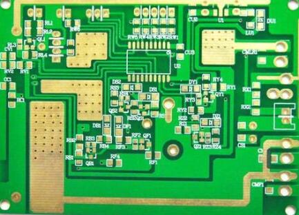
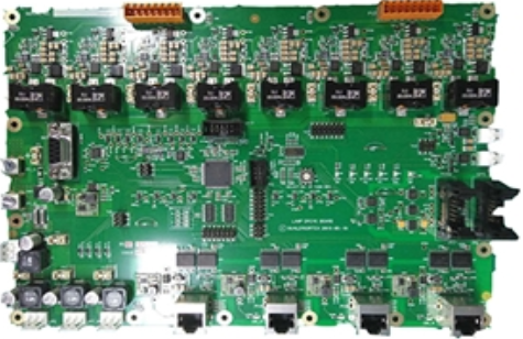
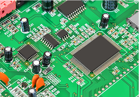
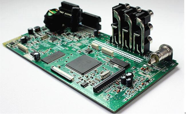
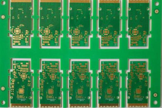
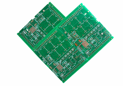
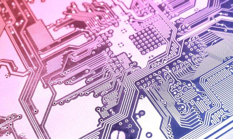
PCB circuit boards are widely used in China. Pollutants will be generated during the manufacturing process of printed circuit boards, including residues of flux and adhesives and other pollutants in the manufacturing process such as dust and debris. If the PCB board cannot effectively guarantee the clean surface, then Resistance and leakage will cause the failure of the PCB circuit board, thereby affecting the service life of the product. Therefore, cleaning the PCB circuit board in the manufacturing process is an important step.
Semi-aqueous cleaning mainly uses organic solvents and deionized water, plus a certain amount of active agent, a cleaning agent composed of additives. This cleaning is between solvent cleaning and water cleaning. These PCB factory cleaning agents are organic solvents and flammable solvents., High flash point, low toxicity, safe to use, but must be washed with water and then dried.

Water purification technology is the development direction of clean technology in the future. It is necessary to establish pure water source and discharge water treatment workshops. Using water as the cleaning medium, surfactants, additives, corrosion inhibitors and chelating agents are added to the water to form a series of Water-based cleaning agent can remove water solvents and non-polar contaminants.
Used in the soldering process without clean flux or clean solder paste, after soldering directly into the next process for cleaning, no longer free cleaning technology is currently the most commonly used alternative PCBA technology, especially mobile communication products are basically disposable The method used instead of ODS, solvent cleaning is mainly used to dissolve and remove pollutants from solvents. Solvent cleaning requires simple equipment due to its fast volatilization and strong solubility.
To make electrical connections between the circuits on both sides of the circuit board, copper has replaced brass as the metal of choice because it can carry current, is relatively low cost and easy to manufacture. In 1956, the United States Patent Office issued a representative of the United States Army. The team of scientists is seeking a patent for the "process of assembling circuits". The patented process for PCB circuit boards involves the use of melamine and other substrates, and a layer of copper foil has been firmly laminated, the wiring diagram is drawn, and then photographed on the zinc board. The plate is used to make the printing plate of the offset printing machine. The acid-resistant ink is printed on the copper foil surface of the circuit board, and the exposed copper is removed by etching, leaving "printed wires". Other methods are also proposed, such as using templates, screening, and handprinting. And rubber stamping to deposit the ink pattern, and then punch the holes with a mold to match the position of the component leads or terminals, insert the leads into the non-plated holes in the laminate, and then immerse or float the card in the molten solder bath. The solder will Cover the traces and connect the leads of the component to the chip factory traces.
Great changes have taken place since then. With the advent of the electroplating process, double-sided PCBs were allowed to appear on the walls of the electroplated holes first. Surface mount technology is a technology that we have associated with the 1980s. It is actually in the past two decades. Research began in the 1960s, and gas masks were applied as early as 1950 to help reduce corrosion that occurred on traces and components. Epoxy compounds are scattered on the surface of the assembly board, similar to the conformal we know now. The coating, which finally screen-prints the ink onto the panel before assembling the printed circuit board, blocks the area to be soldered on the screen.