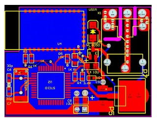
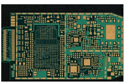
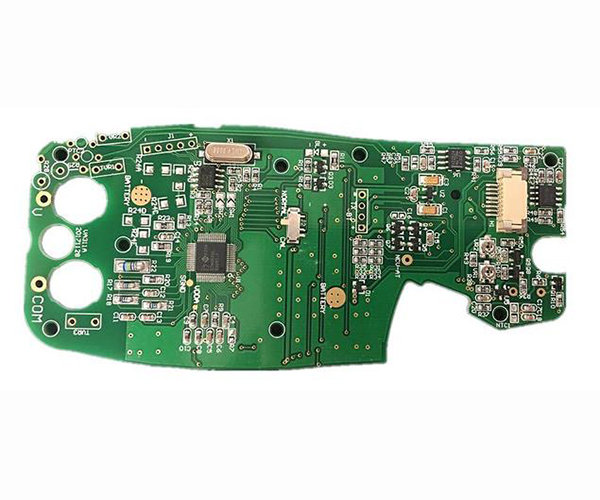
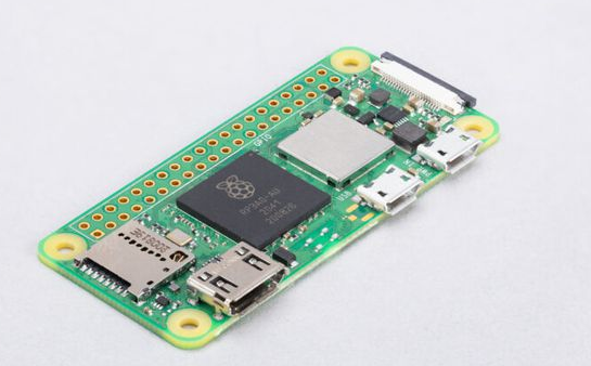
What does PCBA mean? It refers to a series of technological processes from material procurement, PCB production, SMT chip processing, DIP plug-in processing, PCBA testing, and finished product assembly. So what are the welding types of PCBA?
1. What are the welding types of PCBA
1. Reflow soldering
First of all, the first soldering process of PCBA is reflow soldering. After the SMT placement is completed, the PCB board is reflow soldered to complete the soldering of the patch.
2. Wave soldering
Reflow soldering is the soldering of SMD components. For plug-in components, wave soldering is required for soldering. Generally, the PCB board is inserted into the components, and then the plug-in components and the PCB board are welded through the wave furnace.
3. Dip soldering
For some large components, or the influence of other factors, it is not possible to pass wave soldering, so the soldering furnace is often used for soldering. The soldering by the soldering furnace is simple and convenient.
4. Manual welding

Manual soldering means that employees use electric soldering irons for soldering. Generally, manual soldering personnel are required in PCBA processing plants.
PCBA consists of multiple processes, and only through different PCBA welding types can a complete PCBA board be produced.
2. PCBA processing appearance standard
1. Poor contact angle of the solder joint. The wetting angle between the fillet weld and the end joint of the land pattern is greater than 90°.
2. Upright: One end of the component leaves the pad and stands upright or obliquely upward.
3. Short circuit: The solder between two or more solder joints that should not be connected is connected, or the solder of a solder joint is connected with an adjacent wire.
4. Empty soldering: that is, the component leads and the PCB solder joints are not connected by soldering.
5. False soldering: The lead pins of the components and the PCB solder joints seem to be connected, but they are not actually connected.
6. Cold welding: The solder paste at the solder joints is not completely melted or metal alloys are not formed.
7. Less tin (lack of tin consumption): The area or height of tin consumption between the component end and the PAD does not meet the requirements.
8. Too much tin (excess tin): The area or height of the component end and the PAD that eat tin exceeds the requirement.
9. The solder joints are black: the solder joints are black and dull.
10. Oxidation: The surface of components, circuits, PAD or solder joints has produced chemical reactions and colored oxides.
11. Displacement: The component deviates from the predetermined position in the horizontal (horizontal), vertical (vertical) or rotational direction in the plane of the pad (based on the centerline of the component and the centerline of the pad).
12. Polarity reversal (reverse): The direction or polarity of the component with polarity is inconsistent with the requirements of the document (BOM, ECN, component location diagram, etc.).
13. Floating height: There is a gap or height between the components and the PCB.
14. Wrong parts: the component specifications, models, parameters, shape and other requirements are not consistent with (BOM, samples, customer information, etc.).
15. Tin tip: The solder joints of the components are not smooth, and the tip is kept.
16. Multiple pieces: According to BOM and ECN or sample board, etc., there are multiple pieces where parts should not be installed or redundant parts on the PCB.
17. Missing parts: According to BOM and ECN or prototypes, etc., the parts that should be installed on the position or on the PCB but not parts are all missing parts.
18. Dislocation: The position of the component or component pin is moved to the position of other PAD or pin
19. Open circuit (open circuit): PCB circuit disconnection.
20. Side placement (side stand): The chip components with different width and height are placed on the side.
21. Inverted white (turned side): Two symmetrical surfaces with different components are interchangeable (such as: the side with silk-screen logo and the surface without silk-screen logo are upside down), chip resistors are common.
22. Tin beads: small tin spots between the feet of components or outside of the PAD.
23. Air bubbles: There are air bubbles inside solder joints, components or PCB.
24. Tinning (climbing tin): The height of the solder joints of the components exceeds the required height.
25. Tin crack: The solder joint is cracked.
26. Hole plug: PCB plug-in hole or via hole is blocked by solder or other.
27. Damage: cracks or cuts or damages in components, board bottom, board surface, copper foil, circuits, through holes, etc.
28. Blurred silk screen: The text or silk screen of the components or PCB is fuzzy or broken, which can not be recognized or blurred.
29. Dirty: The board surface is not clean, there are foreign objects or stains and other defects.
30. Scratches: PCB or buttons are scratched and copper foil is exposed.
31. Deformation: The components or PCB body or corners are not on the same plane or bent.
32. Blistering (layering) PCB or components are layered with copper and platinum, and there is a gap.
33. Overflowing glue (too much glue) (too much red glue) or overflowing the required range.
34. Little glue (too little amount of red glue) or not up to the required range.
35. Pinhole (concave): PCB, PAD, solder joints, etc. have pinhole concavities.
36. Burr (over the peak): PCB board edge or burr exceeds the required range or length.
37. Impurities of gold finger: There are abnormalities such as pitting, tin spots or solder mask on the surface of gold finger plating.
38. Gold finger scratches: There are scratch marks or bare copper and platinum on the surface of the gold finger plating.
The above is hoped to be helpful to the manufacturers of PCBA processing plants, but the specific situation needs to be analyzed in detail, and the actual situation can be combined with the above to achieve faster quality inspection of PCBA boards.