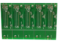
PCB board cutting is an important content in PCB design. But because it involves sandpaper grinding board (belong to harmful work), tracing line (belong to simple and repetitive work), many designers do not want to engage in this work. Even many designers think that PCB cutting is not a technical job, junior designers with a little training can be competent for this job. This concept has som
e universality, but as with many jobs, there are some skills in PCB cutting. If designers master these skills, they can save a lot of time and reduce the amount of labor. Let's talk about this knowledge in detail.

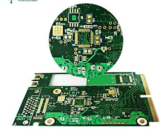
PCB board cutting concept
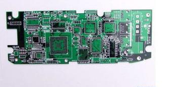
PCB board cutting refers to the process of getting schematic and board drawing (PCB drawing) from the original PCB board. The purpose is to carry out later development. Later development includes installation of components, deep testing, circuit modification, etc. Because it does not belong to the category of PCB board cutting and is related to it, so it is only an introduction and will not be detailed.
PCB board cutting process
1. Remove the devices on the original board.
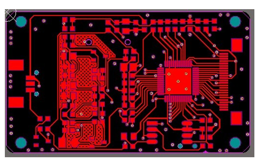
2. Scan the original board to obtain graphic files.
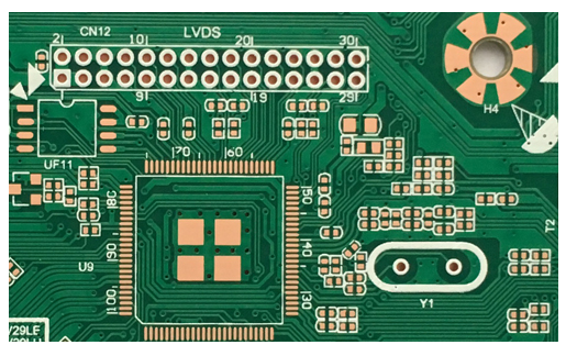
3. Grind off the surface layer to obtain the middle layer.
4. Scan the middle layer to get the graphics file.
5. Repeat steps 2-4 until all layers are processed.
6. Use special software to convert graphics files into electrical relation files -PCB drawings. With the right software, the designer can simply trace the graph.
7. Check and complete the design.
PCB board cutting techniques
PCB board cutting especially multilayer PCB board cutting is a time-consuming and laborious work, which involves a lot of repetitive labor. Designers must be patient and careful enough, otherwise it is very easy to make mistakes. The key of cutting PCB board design is to use suitable software instead of manual repetitive work, which is time saving and accurate.
1. A scanner must be used in the process of dissection.
Many designers are used to drawing lines directly on PCB design systems such as PROTEL, PADSOR or CAD. This habit is very bad. The scanned graphic files are not only the basis for converting into PCB files, but also the basis for later inspection. The use of scanners can greatly reduce the difficulty and intensity of labor. It is no exaggeration to say that, if the scanner can be fully utilized, even people with no design experience can complete the PCB cutting work.
2, single direction grinding plate.
For speed, some designers choose a bidirectional plate (that is, from the front and back surfaces to the middle layer). This is very wrong. Because the two-way grinding plate is very easy to wear, resulting in damage to other layers, the results can be imagined. The outer layer of PCB board is the hardest and the middle layer is the softest due to the process and copper foil and pad. So in the middle layer, the problem is more serious and often cannot be polished. In addition, PCB board produced by various manufacturers are not the same in quality, hardness, elasticity, it is difficult to accurately grind.
3. Choose good conversion software.
Converting the scanned graphics files into PCB files is the key of the whole work. You have good conversion files. Designers simply "follow suit" and sketch the graphics once to complete the work. Here recommend EDA2000, really very convenient.