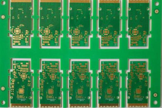
For children’s shoes who are just getting started or just entering the electronic design position, they may get a board and don’t know how to construct a good PCB, or even what the layers are, how to define and distinguish them, let’s take you to uncover the veil of PCB circuit boards. .
Chinese name English name Description Top
(Component layer) Top Layer is mainly used to place components, and can be used for wiring for comparison layer boards and multi-layer boards. Mid Layer can have up to 30 layers. It is used to route signal lines in multi-layer boards. Bottom layer
(Welding layer) Bootom Layer is mainly used for wiring and welding, and sometimes it can also be placed on the top silk screen layer of the component. BottomOverlayer has the same function as the top silk screen layer. If various labels are included on the top silk screen layer, then the bottom silk screen layer does not need the internal power ground layer. Internal Planes Mechanical Layers Mechanical Layers The mechanical layer defines the appearance of the entire PCB board. Generally used to set the external dimensions of the circuit board, data marks, alignment marks, assembly instructions and other mechanical information. Solder mask

(Main soldering layer) Solder Mask has two layers: Top solder Mask and Bootom Solder mask. It is the board layer protection automatically generated by ProtelPCB corresponding to the pad and via data in the circuit board file. Solder paste layer
(SMD patch layer) There are two layers: Top PastMask and Bottom Pastmask. It is used to correspond to the solder joints of SMD components when the soldering furnace is used. It is also a negative film output that prohibits wiring. The layer Keep Ou Layer defines the boundary of the wiring layer. After the forbidden wiring layer is defined, in the subsequent wiring process, the wiring with electrical characteristics must not exceed the boundary of the forbidden wiring layer. Multilayer MultiLayer refers to all layers of the PCB board. The pads and penetrating vias on the circuit board should penetrate the entire circuit board and establish electrical connections with different conductive pattern layers. NC drilling layer NC Drill drilling reference layer Drill Drawing
Signal Layers: Signal layers include Top Layer, Bottom Layer, and Mid Layer 1…30. These layers are all layers with electrical connections, that is, the actual copper layer. The middle layer refers to the middle board layer used for wiring, and the wires are distributed in this layer. Top Layer
The top signal layer (Top Layer), also known as the component layer, is mainly used to place components. For double-layer boards and multilayer boards, it can be used to arrange wires or copper. The bottom signal layer (Bottom Layer), also known as the soldering layer, is mainly used for wiring and soldering. It can be used to place components for double-layer boards and multilayer boards. The middle signal layer (Mid-Layers) can have up to 30 layers, which are used to arrange signal lines in a multi-layer board. Power lines and ground lines are not included here.
Internal Plane: Internal Plane 1...16. This type of layer is only used for multilayer boards. These layers are generally connected to the ground and power supply and become the power supply layer and the ground layer. They also have electrical connections and are also actual copper. Layer, but this layer is generally not wired and is composed of a whole piece of copper film.
Usually referred to as the inner electric layer for short, it only appears in multi-layer boards. The number of PCB board layers generally refers to the sum of the signal layer and the inner electric layer. Same as the signal layer, the inner electric layer and the inner electric layer, and the inner electric layer and the signal layer can be connected to each other through through holes, blind holes and buried holes.
Silkscreen Overlay: Including the top silkscreen overlay and the bottom silkscreen overlay. The silk screen characters that define the top and bottom layers are generally some text symbols printed on the solder mask, such as component names, component symbols, component pins, copyrights, etc., to facilitate future circuit soldering and error checking.
A PCB board can have up to 2 silk screen layers, namely the top silk screen layer (Top Overlay) and the bottom silk screen layer (Bottom Overlay), generally white, mainly used to place printed information, such as the outline and labeling of components, each A kind of comment characters, etc., to facilitate the soldering of PCB components and circuit inspection. The top silk screen layer (Top Overlay) is used to mark the projection outline of the component, the label, the nominal value or model of the component, and various annotation characters. The bottom silk screen layer (Bottom Overlay) is the same as the top silk screen layer. If all the labels on the top silk screen layer are included, the bottom silk screen layer can be closed.
Paste Mask: or soldering layer, including the top layer of solder paste (Top paste) and the bottom layer of solder paste (Bottom paste), refers to the exposed surface mount pads that we can see, also It is the part that needs to be coated with solder paste before soldering. Therefore, this layer is also useful for hot air leveling of the pads and the production of welded steel mesh.
Mechanical Layers: Up to 16 mechanical processing layers can be selected. To design a double panel, you only need to use the default option Mechanical Layer 1. The mechanical layer defines the appearance of the entire PCB board. It is generally used to place indicative information about the manufacturing and assembly methods, such as the outline size of the PCB, size markings, data materials, via information, assembly instructions and other information. Designed as a PCB mechanical shape, the default LAYER1 is the shape layer. Other LAYER2/3/4, etc. can be used for mechanical size marking or special purposes. For example, when certain boards need to be made of conductive carbon oil, LAYER2/3/4, etc. can be used, but the purpose of the layer must be clearly marked on the same layer.