1. The definition of processing level is not clear
Single panel PCB design in the TOP layer, if not specified positive and negative, may be produced by the board mounted on the device and not good welding.
2. A large area of copper foil is too close to the outer frame
The distance between large copper foil and the outer frame should be at least 0.2mm, because when milling out the shape, such as milling to the copper foil is easy to cause the copper foil warping and caused by it solder resistance shedding problem.
3. Draw the pad with the filling block
Drawing pads with filler blocks can pass DRC inspection in circuit design, but not in processing. Therefore, solder block class CAN not directly generate solder blocking data. When solder blocking agent is applied, the filling block area will be covered by solder blocking agent, resulting in difficulty in device welding.

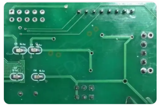
4. The electric formation is also the flower pad is also the connection
Because of the design of flower pad power supply, the stratum is opposite to the actual printed board as shown in the figure above. All the lines are isolation lines. When drawing several sets of power supply or several kinds of ground isolation lines, care should be taken not to leave gaps, short-circuit the two sets of power supply, nor cause the connection area to be blocked.
5. Characters misplaced
Character cover pad SMD weld plate, PCB on/off test and component welding inconvenience. The character design is too small, which makes screen printing difficult, and too large, which makes characters overlap and difficult to distinguish.
6. Surface mount device pad is too short
This is for the on-off test, for too dense surface mount device, the spacing between the feet is quite small, the pad is also quite fine, the installation of the test needle, must be staggered, such as pad design is too short, although it does not affect the device installation, but will make the test needle is not wrong.
7. Single-sided pad aperture setting
Single-sided pads generally do not drill holes, if drilling holes need to be marked, the aperture should be designed as zero. If a value is designed so that the hole coordinates appear at this location when the borehole data is generated, the problem arises. Single side pads should be specially marked as drilling holes.
8. Pad overlap
In the drilling process, the drill bit will be broken because of drilling multiple times in one place, resulting in hole damage. The two holes in the multilayer plate overlap, and the negative is drawn as an isolation plate, resulting in scrap.
9. Too many filling blocks in the design or filling blocks with extremely thin lines
The optical drawing data is lost, and the optical drawing data is incomplete. Because filling blocks are drawn one by one in light drawing data processing, the amount of light drawing data is quite large, which increases the difficulty of data processing.
10. Graphic layer abuse
Some useless lines were made on some graphic layers, and more than five lines were designed for four layers, which caused misunderstanding. Violate conventional design. Keep the graphics layer complete and clear when designing