When designing a circuit board with PCB proofing, the circuit principle design is very good, or even very good, but various noises will appear during the debugging process, and the circuit board cannot achieve the expected purpose, sometimes more, and the board has to be re-made.
So how to reduce PCB noise? Let's analyze it. For a circuit board with good performance, we electronic engineers can see its general distribution at a glance (as long as they know what the circuit board can do), this is what we usually call the principle of separation of functional modules. The functional module is composed of multiple electronic components to complete certain functions of the circuit group. In actual design, we need to be close to these electronic components to reduce the wiring length between the electronic components to increase the role of the circuit module.
In fact, it is not difficult to understand that our common development boards or mobile phones do this, especially mobile phones. If you separate the mobile phones, you will find that the separation between the modules is obvious. Each module is used through a Faraday cage. shield.

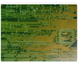
How to reduce the noise of the circuit board. The above is the development board of the PCB. It can be seen from the layout that the separation of the interface circuit is clear, and the wiring of SDRAM, DDR and SD card interface circuit will not cause mutual interference.
By dividing system modules, it helps signal integrity, prevents high-frequency interference between system modules, and improves system stability. Secondly, it should also be noted that when there are analog and digital circuits on the PCB circuit board, the two must be separated. If the cap must be put on, there is a silent area. The so-called silent area is an area where analog and digital circuits or functional modules are physically separated. In this way, you can prevent other modules from interfering with the module. In the mobile circuit board mentioned above, the silent zone is obvious.
Please note that the silent area and the ground of the circuit board are not connected.
In the actual PCB proofing circuit design, not every PCB board has enough space for us to make a silent area, then, when no space is allowed, how should we design it?
A, use transformers or signal isolation components for design.
It is precisely this meaning that we often use circuit separation composed of components such as CMOS or transistors.
B, the signal enters the module before passing through the filter circuit.
This method is a common method to prevent ESD, and it is also considered that this method can play a role in eliminating noise (ESD, high frequency and high voltage noise).
C. Use common mode inductors for signal protection. If we don't know the role of common mode inductance, we will find that there are only two coils in the schematic diagram, and the effect is not great. In fact, this plays an important role in the stability of the signal and the elimination of noise interference.
On the other hand, PCB proofing also reveals that it takes a long time for electronic engineers to grow. A method similar to the silent area of circuit board design is trench protection technology. This technology is a technology that removes the segmented copper skin from the silent area and forms the exposed circuit board material. The concept of the bridge originates from this: the power, ground and signal lines that connect the various parts together are called bridges.
The trench technology is resistant to the impact of peak voltage and classic discharge protection carrying capacity, and to a certain extent, it can reduce the noise of the circuit board.
In PCB design, routing through trenches that are not related to the isolation area will generate RF loop current, but it will affect the performance of the circuit board. This requires attention. Now, many analog-to-digital or digital-to-analog components have been connected together in the two parts of the ground, usually ADC and DAC devices. These devices must be segmented and have a standard reference position. If the digital signal current Can not effectively return to the source, it will produce noise and generate EMI. When drawing the schematic, we found that the agnd and DGND pins are devices with superior performance, which will reduce the difficulty of our design. Usually, the PCB proofing circuit is partitioned according to the module, and the obvious static area between the partitions is designed to minimize the influence of power and ground on the signal, thereby minimizing the noise of the circuit board.