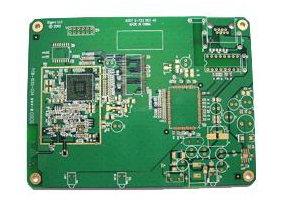
At present, high-frequency and high-speed PCB design has become the mainstream, and every PCB Layout engineer should be proficient. Next, Banermei will share with you some of the design experience of hardware experts in high-frequency and high-speed PCB circuits, and I hope it will be helpful to everyone.
1. How to avoid high frequency interference?
The basic idea of avoiding high-frequency interference is to minimize the electromagnetic field interference of high-frequency signals, which is the so-called crosstalk (Crosstalk). You can increase the distance between the high-speed signal and the analog signal, or add ground guard/shunt traces next to the analog signal. Also pay attention to the noise interference from the digital ground to the analog ground.
2. How to consider impedance matching when designing high-speed PCB design schematics?

When designing high-speed PCB circuits, impedance matching is one of the design elements. The impedance value has an absolute relationship with the wiring method, such as walking on the surface layer (microstrip) or inner layer (stripline/double stripline), distance from the reference layer (power layer or ground layer), wiring width, PCB material, etc. Both will affect the characteristic impedance value of the trace. That is to say, the impedance value can only be determined after wiring. Generally, simulation software cannot take into account some wiring conditions with discontinuous impedance due to the limitation of the circuit model or the mathematical algorithm used. At this time, only some terminators (termination), such as series resistance, can be reserved on the schematic diagram. Alleviate the effect of discontinuity in trace impedance. The real solution to the problem is to try to avoid impedance discontinuities when wiring.
3. In high-speed PCB design, which aspects should the designer consider EMC and EMI rules?
Generally, EMI/EMC design needs to consider both radiated and conducted aspects at the same time. The former belongs to the higher frequency part (<30MHz) and the latter is the lower frequency part (<30MHz). So you can't just pay attention to the high frequency and ignore the low frequency part. A good EMI/EMC design must take into account the location of the device, PCB stack arrangement, important connection method, device selection, etc. at the beginning of the layout. If there is no better arrangement beforehand, it will be resolved afterwards. It will do twice the result with half the effort and increase the cost. For example, the location of the clock generator should not be as close to the external connector as possible. High-speed signals should go to the inner layer as much as possible. Pay attention to the characteristic impedance matching and the continuity of the reference layer to reduce reflections. The slew rate of the signal pushed by the device should be as small as possible to reduce the height. Frequency components, when choosing a decoupling/bypass capacitor, pay attention to whether its frequency response meets the requirements to reduce noise on the power plane. In addition, pay attention to the return path of high-frequency signal current to make the loop area as small as possible (that is, loop impedance as small as possible) to reduce radiation. The ground can also be divided to control the range of high-frequency noise. Finally, properly choose the chassis ground between the PCB and the housing.
4. How to choose PCB board?
The choice of PCB board must strike a balance between meeting design requirements and mass production and cost. The design requirements include both electrical and mechanical parts. Usually this material problem is more important when designing very high-speed PCB boards (frequency greater than GHz). For example, the commonly used FR-4 material, the dielectric loss at a frequency of several GHz will have a great influence on the signal attenuation, and may not be suitable. As far as electricity is concerned, pay attention to whether the dielectric constant and dielectric loss are suitable for the designed frequency.
5. How to meet EMC requirements as much as possible without causing too much cost pressure?
The increased cost of PCB circuit board due to EMC is usually due to the increase of the number of ground layers to enhance the shielding effect and the addition of ferrite bead, choke and other high-frequency harmonic suppression devices. In addition, it is usually necessary to match the shielding structure on other institutions to make the entire system pass the EMC requirements.