Traditional PCB design is often divided into so-called single and double panels and multi-layer boards, and multi-layer boards are divided into single-press and multiple-press geometric structures. Of course, such a design involves some electrical properties and connection density issues, but the more important issue is that it is limited by the precision of electronic product manufacturing technology. These geometric structures can no longer meet the mounting density and electrical characteristics of electronic components.
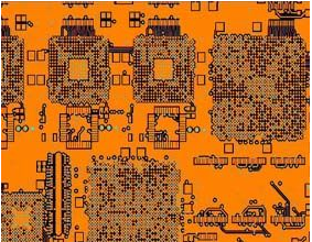
In order to increase the connection density of components, from a geometric point of view, only by compressing the space between the circuit and the connection point and allowing more contacts to be accommodated in a smaller space can the connection density be increased. Of course, there is another different idea, that is, multiple different components can be stacked in the same position to increase the density of the structure. Therefore, from a certain point of view, high-density circuit boards are not only a technical problem of circuit boards, but also a problem of electronic construction and assembly. I am afraid that this aspect is worthy of the industry's efforts to understand. Figure 1.1 shows the demand for high-density technology for general 3C products.

Why do you need a high-density PCB circuit board
The so-called electronic package generally refers to the connection relationship between the semiconductor chip and the carrier board. In this regard, the Civil Road Board Association has published a book on "Electronic Structure Loading Board Technology", and those who are interested can refer to it. As for the electronic assembly part, it is the work of reinstalling the components after the electronic assembly is completed on another functional circuit board. This connection is generally called OLB (outer lead bond), which refers to the connection part of the external lead of the component. The connection of this part is directly related to the surface contact density of electronic components. When the functions and integration of electronic products are getting higher and higher, and at the same time, the demand for mobility, thinness, and multi-function continues to increase., Of course, there will be high-density pressure.
If the design concept of high-density PCB circuit board is adopted, electronic products can basically get the following benefits:
1. The number of layers of the carrier can be reduced, and the more traditional and complex structures can be made with this technology to reduce product costs.
2. Increase the line density, and hide the wiring required for interconnection to the next layer with microvia technology. The connection between the pads and leads between different layers is performed in a direct connection mode designed with a combination of pads and blind holes. This can meet the component assembly requirements of high-density contacts, which is conducive to the use of advanced packaging technology.
3. The use of microvia interconnection can reduce signal reflection and cross-talk interference between lines, and components can have better electrical performance and signal accuracy.
4. The structure adopts a thinner dielectric thickness, and the micro-holes have a low aspect ratio, and the reliability of signal transmission is higher than that of ordinary through-holes.
5. The micro-hole technology allows the carrier board designer to shorten the distance between the ground layer and the signal layer, reduce radio frequency interference and electromagnetic wave interference, thereby improving radio frequency interference / electromagnetic wave interference / electrostatic discharge. At the same time, the number of grounding wires can be increased to prevent components from being damaged by instantaneous discharge caused by static electricity accumulation.
6. The microporous technology can make the circuit configuration flexible and make the circuit design flexible.
Some people joked that modernity is a crazy generation. Not only do electronic products need to be mobile, they must also be worn without burdens, but they must also look good. Of course, the most important thing is that the products are cheap and can be replaced with fashion. If there is not much financial burden.
There are a lot of new business behavior rules, creating new ways to play in different fields, among which the most noticed is the so-called one-dollar mobile phone or free electronic goods. How to meet the trend, light and thin, and how to obtain commercial benefits at a low unit price or even as a gift, these must be high-tech but low-cost capabilities to deal with. Of course, the important electronic component carrier PCB circuit board is no exception, this is an obvious trend of mobile electronics.