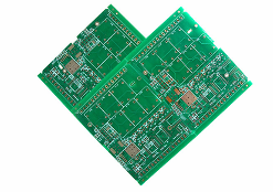
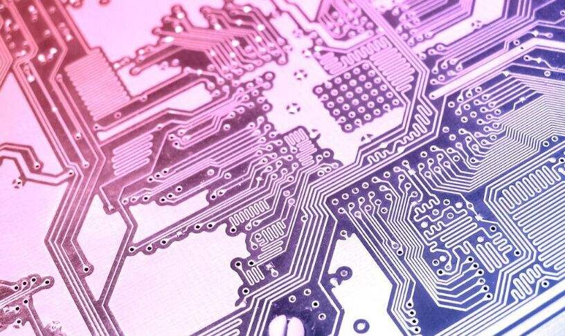
The following is an introduction to the ENIG surface treatment of PCB circuit boards:
ENIG (Electroless Nickel Immersion Gold, Electroless Nickel Immersion Gold) is a process used for the surface treatment of circuit boards (Finished). It is generally referred to as "nickel immersion gold plate" or "nickel immersion gold plate" for short. It is widely used on circuit boards installed in mobile phones, and some BGA carrier boards also use ENIG.
Compared with electroplated nickel gold, this kind of nickel immersion gold does not need to be energized on the circuit board during the process of the circuit board factory, nor does it need to pull a wire on each pad to be electroplated to be plated with nickel. Gold, so its manufacturing process is relatively simple, and the output is more than multiple, so the production cost is relatively cheap.
However, ENIG surface treatment also has its shortcomings and problems. For example, the welding strength is low and black pads are easily formed, which are often criticized.
ENIGPCB
The production process of chemical nickel gold is roughly as follows:

Pretreatment - degreasing - water washing - pickling - water washing - micro-etching - water washing - pre-dipping (H2SO4) - activation (Pd catalyst) - water washing - chemical nickel (Ni/P) - water washing - immersion gold plating - gold recovery - water washing - drying
Pre-treatment: The purpose is to brush or sandblast to remove oxides on the copper surface and roughen the copper surface to increase the subsequent adhesion of nickel and gold.
Micro-etching: sodium persulfate/sulfuric acid to remove the oxide layer on the copper surface and reduce the depth of groove marks caused by brushing during pretreatment. Too deep brush marks often become an accomplice of the immersion gold attacking the nickel layer.
Activation: Since the copper surface cannot directly initiate the chemical nickel deposition reaction, a layer of palladium (Pd) must be applied to the copper surface as a catalyst for the chemical nickel deposition reaction. Using the principle that Cu is more active than Pd, palladium ions are reduced to palladium metal and attached to the copper surface.
Chemical nickel: Ni/P, its main function is to prevent the migration and diffusion between copper and gold, and as an element that chemically reacts with tin to generate IMC during subsequent welding.
Dip gold plating: The main purpose of gold is to protect and prevent the oxidation of the nickel layer. Gold does not participate in the chemical reaction during the soldering process. Too much gold will hinder the strength of the solder, so gold only needs to cover the nickel layer to make it difficult Oxidation is sufficient, if COB (Chip On Board) wiring is to be used, it is another matter, because the gold layer must have sufficient thickness.
Advantages of PCBENIG (nickel immersion gold) surface treatment:
Its surface treatment can be used as the bottom metal of COB wire bonding.
It can be repeatedly reflowed (reflow), and it is generally required to be able to withstand at least 3 times of high temperature welding, and the welding quality can still be maintained.
Has excellent electrical conductivity. It can be used as a golden finger circuit for button conduction, and it has high reliability.
Gold metal has low activity and is not easy to react with the components in the atmosphere, so it can play a certain degree of anti-oxidation and anti-rust ability. Therefore, the shelf life of ENIG can generally easily exceed six months. Sometimes even if it is stored in the warehouse for more than one year, as long as it is kept in good condition and there is no rust problem, the circuit board is baked, dehumidified and soldered after testing. It is confirmed that there is no problem, and it can still be used for welding production.
Gold is not easy to oxidize when exposed to the air, so a large area of exposed pad can be designed for "heat dissipation".
It can be used as the contact surface of the blade. The gold layer for this application must be thicker. Hard gold plating is generally recommended.
The surface of ENIG is flat, the flatness of printed solder paste is good, and it is easy to solder. It is very suitable for fine inter-foot parts and small parts, such as BGA, Flip-Chip and other parts.
Disadvantages of PCBENIG surface treatment:
Generally speaking, the solder joint strength of Ni3Sn4 is not as good as that of Cu6Sn5, and some parts that require soldering strength may not be able to withstand excessive external impact and risk of falling.
Because the price of "gold" is rising steadily, the cost is relatively higher than that of OSP surface treatment.
There is a risk of "black pad" or "black nickel". Once the black pad is generated, it will cause the problem of a rapid decrease in the strength of the solder joint. The black pad is composed of a complex NixOy chemical formula. The fundamental reason is that the nickel surface undergoes excessive oxidation reaction during the immersion gold substitution reaction on the nickel surface (metal nickel becomes nickel ions, which can be called oxidation in a broad sense). In addition to the irregular deposition of very large gold atoms (gold atom radius 144pm) to form a rough and loose porous grain arrangement, that is to say, the "gold" layer cannot completely cover the "nickel" layer underneath, giving the nickel layer a chance Continue to contact with air, and finally nickel rust will gradually form under the gold layer, which will eventually hinder welding. There is a process called "Nickel-Immersed Palladium Gold ((ENEPIG)") that can effectively solve the "black pad" problem, but because its cost is still relatively expensive, it is currently only used by high-end board, CSP or BGA companies.