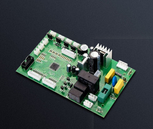
What is a compound fixture? How is it different from Dedicated fixture & Universal fixture? Can it effectively reduce the test cost of the circuit board factory? Will it affect the reliability of the test results? How is Fixture made? What about its future development?
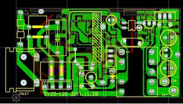
The traditional circuit board design is based on the assembly of through-hole parts, so the pin distance is also designed based on this type of parts as the circuit board contact spacing. In the past, the typical lead distance was divided into ten parts per inch, so the lead distance is about one contact per 100 mils. If the coordinates of the circuit board are marked, with 100 mils per grid as the unit, the checkerboard cross grid points can be determined on the circuit board surface, and these cross grid points are called Grid.
If all the electronic component contacts are designed on the grid point, it is an On Grid design. The On Grid fixture used to test this kind of circuit board is called the Universal fixture. Because the jig probe holes are all equipped with fixed grid points, the test jig can be reused as long as the probe is reconfigured. This is the source of the Universal name. Using this type of fixture can certainly reduce costs.

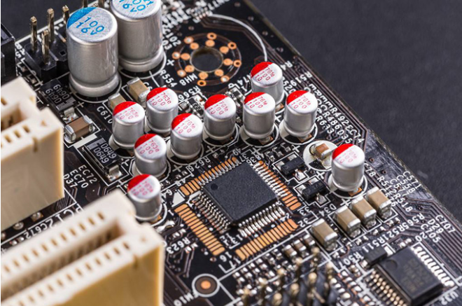
However, electronic parts are gradually turning to surface mount (SMD) design. At present, the contact density of electronic products has been greatly improved, especially the array design has been adopted for most of the contact configurations. Therefore, the traditionally used Universal test fixtures can no longer meet this high density. Test requirements. At this time, double-density and four-density dial tests appeared, and this type of density fixture is still called Universal fixture.
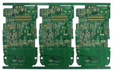
If the high-density PCB circuit configuration cannot be tested with Universal fixtures, special fixtures must be made for specific needs. This fixture is Dedicate Fixture. Using this kind of jig, of course, the test density and ability can be improved, but the production cost is not cheap, and the design and difficulty of the test jig will be higher.
The so-called composite jig is to use two different jigs in combination. This is the current testing method for most circuit boards, which can take into account the dual requirements of cost and test capability. Basically, these testing methods are still based on contact testing, so there should be no problem with reliability. Dedicate fixtures are difficult to manufacture because of the high probe density. At the same time, because of the high unit price of probes, the fixtures cannot be reused, so the production costs are spent on probes and special fixtures.
At present, there are many researches towards the development of non-contact testing methods. However, because there are not many users and there is still a risk of missed testing so far, the current electrical testing method in the industry is still the mainstream of the contact type. As for a small number of diversified products, some companies also use flying probe testers to test. High-speed flying probes and non-contact electrical testing methods are still the future direction that the industry strives to achieve.