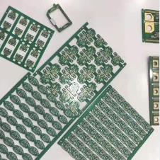
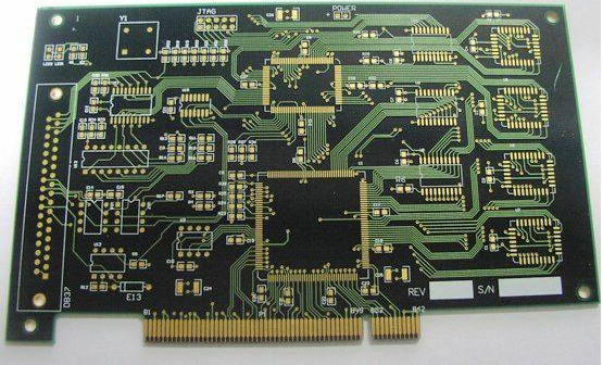
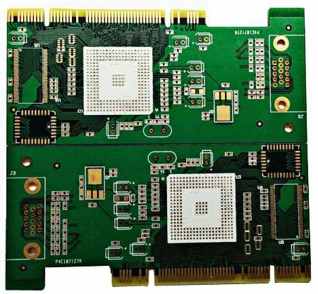
PCB circuit board design-substrate design principles are as follows:
1. In the substrate, the pad of the DIE must be in the same direction as the bonding wire, and the lead wire must also be in the same direction as the pad. For each DIE, a cross-shaped pad must be placed on its diagonal. As the alignment coordinates when binding, the coordinates need to be connected to the network of the attachment. Generally, the location is selected (the network must be present, otherwise the cross will not appear), and in order to prevent the cross from being submerged by the copper, it is generally used It is forbidden to lay copper plates to surround it.
For the binding of DIE, note that the unused pads, that is, the pads that are not connected to the network, need to be deleted.
2. The production process of the substrate is special, and each line must be made of electroplated lines to form copper materials by electroplating to form pads and traces, or all other places where copper is needed. It must be noted here that even if there is no electrical connection, that is, no network, the pad must be pulled out of the board frame to plate the pad with copper in the eco mode, otherwise the pad will be copper-free.

And the electroplated wire drawn out of the board frame must have a copper skin on the other layer to mark its corrosion position, here is the seventh layer of copper skin. Generally speaking, the copper sheet is 0.15mm beyond the inner side of the board frame, and the distance between the copper-laid edge and the board frame is about 0.2mm.
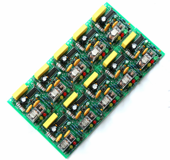
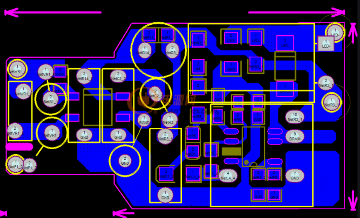
3. In the board frame, to determine the positive and negative, it is best to place all the components on the same side, which is marked with three XXX, as shown in the figure below.
4. The pad used on the substrate is larger than the general pad and has a special package, which is CX0201. The X mark is different from C0201. Organized as follows:
0603 pad: 1.02mmX0.92mm open window area of the pad: 0.9mmX0.8mm, the distance between the two pads is 1.5mm.
0402 pad: 0.62mmX0.62mm pad window area: 0.5mmX0.5mm, the distance between the two pads is 1.0mm.
0201 pad: 0.42mmX0.42mm pad window area: 0.3mmX0.3mm, the distance between the two pads is 0.55mm.
5. The requirements of DIE are as follows: the minimum size of bonding pads (single wire) is 0.2mmX0.09mm90 degrees, the spacing of each pad is at least 2MILS, and the pad width of the inner row of ground and power lines is also required to be 0.2 mm. The angle of the bonding pad should be adjusted according to the angle of the component pulling wire. When making the substrate, the binding wire is not easy to be too long. The minimum distance between the main control DIE and the inner bonding pad is 0.4mm, and the minimum distance between the FLASHDIE and the bonding pad is 0.2mm. The longest binding wire between the two should not exceed 3mm. The spacing between the two rows of bonding pads should be more than 0.27mm apart.
6. The distance between the SMT pad and the DIE bonding pad and the SMT component should be kept above 0.3mm, and the distance between the bonding pad of one DIE and the other DIE should also be kept above 0.2mm. The minimum signal trace is 2MILS, and the spacing is 2MILS. The main power line is best to be 6-8MILS, and try to spread the ground in a large area. Where it is not possible to lay the ground, power and other signal lines can be laid to enhance the strength of the substrate.
7. Pay attention to the vias and pads when the PCB wiring. The gold fingers should not be too close to each other. The vias and gold fingers of the same attribute should be kept at least 0.12mm, and the vias with different attributes should be kept as far away as possible from the pad and Gold finger. The minimum via hole is 0.35mm for the outer hole and 0.2mm for the inner hole. When laying copper, pay attention to the copper and the gold fingers not to be very close, and some broken copper should be deleted, and it is not allowed to have a large area that is not covered. Where copper exists.
8. Grid should be used when PCB copper is laid. The ratio is 1:4, which means that the copper pour angle of COPPERPOUR is 0.1mm and COPPER is 0.4mm instead of 45 degrees.