The position of PCB passive components in the entire electronics industry is the same as that of ICs. They are located upstream and are essential components in electronic products. Electronic circuits have active and passive devices. The so-called passive components can operate without being connected to electricity, and produce functions such as regulating current and voltage, storing static electricity, preventing electromagnetic interference, and filtering current impurities.
Compared with the active component, when the voltage of the passive component changes, the resistance and impedance will not change with it.
Passive components can cover three categories of products: resistors, inductors and capacitors.
Traditionally, EMC has been regarded as "black magic". In fact, EMC can be understood by mathematical formulas. However, even if there are mathematical analysis methods available, those mathematical equations are still too complicated for actual EMC circuit design. Fortunately, in most practical work, engineers do not need to fully understand those complicated mathematical formulas and the theoretical basis existing in EMC specifications. As long as they use simple mathematical models, they can understand how to meet EMC requirements. .
This article uses simple mathematical formulas and electromagnetic theory to illustrate the hidden behaviors and characteristics of passive components on printed circuit boards (PCBs). These are the requirements that engineers have to design beforehand when they want to make their electronic products pass EMC standards. Must have basic knowledge.

1. Wire and PCB trace
The seemingly inconspicuous components such as wires, traces, fixing frames, etc. often become the best transmitters of radio frequency energy (that is, the source of EMI). Every component has an inductance, which includes the bond wires of the silicon chip, and the pins of resistors, capacitors, and inductors. Each wire or trace contains hidden parasitic capacitance and inductance. These parasitic components will affect the impedance of the wire and are very sensitive to frequency. According to the value of LC (which determines the self-resonance frequency) and the length of the PCB trace, self-resonance (self-resonance) can be generated between a component and the PCB trace, thus forming an efficient radiating antenna.
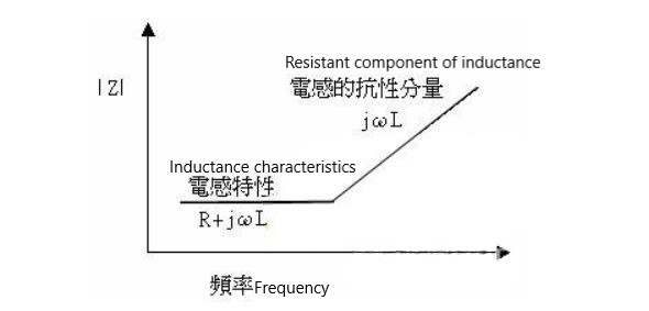
At low frequencies, the wire generally only has the characteristics of resistance. But at high frequencies, the wire has the characteristics of inductance. Because it becomes high frequency, it will cause the change of impedance, and then change the EMC design between the wire or PCB trace and the ground. At this time, the ground plane and ground grid must be used.
The main difference between wires and PCB traces is that the wires are round and the traces are rectangular. The impedance of a wire or trace includes resistance R and inductance XL = 2πfL. At high frequencies, this impedance is defined as Z = R + j XL j2πfL, and there is no capacitive reactance Xc = 1/2πfC. When the frequency is higher than 100 kHz, the inductance is greater than the resistance. At this time, the wire or trace is no longer a low-resistance connecting wire, but an inductance. Generally speaking, wires or traces that work above audio frequency should be regarded as inductance, and can no longer be regarded as resistance, and can be a radio frequency antenna.
The length of most antennas is equal to 1/4 or 1/2 wavelength (λ) of a certain frequency. Therefore, in the EMC specification, wires or traces are not allowed to work below λ/20 of a certain frequency, because this will suddenly turn it into a high-performance antenna. Inductance and capacitance will cause the resonance of the circuit, this phenomenon will not be recorded in their specifications.
For example: Suppose there is a 10 cm trace, R = 57 mΩ, 8 nH/cm, so the total inductance value is 80 nH. At 100 kHz, an inductive reactance of 50 mΩ can be obtained. When the frequency exceeds 100 kHz, this trace will become an inductance, and its resistance value can be ignored. Therefore, this 10 cm trace will form an efficient radiating antenna when the frequency exceeds 150 MHz. Because at 150 MHz, its wavelength λ = 2 meters, so λ/20 = 10 cm = the length of the trace; if the frequency is greater than 150 MHz, its wavelength λ will be smaller, and its 1/4λ or 1/2λ value will be It is close to the length of the trace (10 cm), so a perfect antenna is gradually formed.
2. Resistance
Resistor is the most common component found on PCB. The material of the resistor (carbon synthesis, carbon film, mica, winding type... etc.) limits the effect of frequency response and the effect of EMC. Wire-wound resistors are not suitable for high-frequency applications because there is too much inductance in the wires. Although carbon film resistors contain inductance, they are sometimes suitable for high-frequency applications because the inductance of its pins is not large.
Three, PCB capacitance
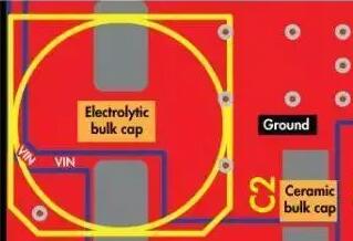
Capacitors are generally used in the power bus to provide decouple, bypass, and maintain a fixed DC voltage and current (bulk) functions. A truly pure capacitor will maintain its capacitance value until it reaches the self-resonant frequency. Beyond this self-resonance frequency, the capacitance characteristics will become like an inductance. This can be explained by the formula: Xc=1/2πfC, Xc is capacitive reactance (unit is Ω). For example: a 10μf electrolytic capacitor, at 10 kHz, the capacitive reactance is 1.6Ω; at 100 MHz, it drops to 160μΩ. Therefore, at 100 MHz, there is a short circuit effect, which is ideal for EMC. However, the electrical parameters of electrolytic capacitors: equivalent series inductance (ESL) and equivalent series resistance (ESR), will limit this capacitor to only work at frequencies below 1 MHz.
The use of PCB capacitors is also related to the pin inductance and volume structure. These factors determine the number and size of parasitic inductances. Parasitic inductance exists between the welding wires of the capacitor. They cause the capacitor to behave like an inductance when it exceeds the self-resonance frequency. Therefore, the capacitor loses its original function.