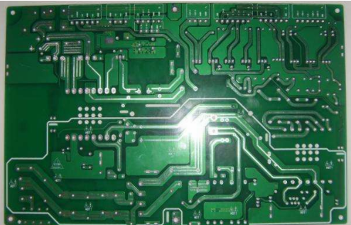
With the continuous development of electronic products, customers have more and more diversified requirements for the metallized half-holes on the side of the PCB. At the same time, the quality of the metallized half-holes on the side of the PCB directly affects the installation and use of customers. This article uses secondary molding and secondary drilling to process the metallized half-holes the PCB side, and elaborates the skills and control methods in the process of metallized half-holes on the side of the PCB.
1 Introduction:
The semi-metallized hole process on the side of the finished PCB is already a mature process in PCB processing, but how to control the product quality after the semi-metallized hole on the side of the PCB is formed: such as the copper thorns on the hole wall and the residue has always been a mechanical processing process A difficult problem in. This kind of PCB with a whole row of semi-metallized holes on the side of the PCB is characterized by relatively small individuals. Most of them are used on the PCB board, as a daughter PCB of a mother PCB board, through these semi-metallized holes and the mother PCB board And the pins of the components are soldered together. Therefore, if there are copper thorns remaining in these semi-metallized holes, when the plug-in manufacturer performs soldering, it will cause weak solder feet and false soldering, which will seriously cause a bridge short circuit between the two pins. This article mainly focuses on the problems encountered in the process of PCB board edge metallization half-hole processing and how to control and ensure the demonstration.
2. Principle of mechanical processing:

Whether it is drilling or milling, the direction of rotation of the SPINDLE is clockwise. When the tool is processed to point A, since the metallization layer of the hole wall at point A is closely connected with the base material layer, it can prevent the metallization layer from being The extension during processing and the separation of the metallization layer from the hole wall will also ensure that the copper thorns will not be lifted or left after processing. When the tool is processed to point B, due to the copper attached to the hole wall Without any support from the schematic diagram of Figure 1, when the tool moves forward, the metalized layer in the hole will curl with the direction of rotation of the tool under the influence of external force, causing copper thorns to lift and remain.
3. PCB side half hole product type:
4. Problems in processing and improvement methods:
Our common types can be divided into the above four types. In the processing of these four types, we have adopted two methods:
4.1 Type 1 and Type 2 are products with a larger half-hole spacing. We adopt the processing method of double milling on the front and back:
Because the user designed the half-hole spacing of this type of product to be greater than 3mm, the metalized half-hole can be processed from one side of the CS surface by milling in the first step, and then the product is turned over in the second step and then processed on the other side of the SS surface. During the forward/reverse processing, the two different stress points on the side of the PCB do not affect each other, and the processed half-holes are smooth and tidy. Such products are relatively simple in processing and easy to guarantee.
4.2 Type 3 and Type 4 belong to the half hole whose diameter is less than 0.8mm, and the center distance of the two half holes is also about 1mm, and the distance between the half holes of two adjacent rows is not more than 2.5mm. Between half holes and on both sides. Encountered the following problems during the processing: After processing, the product has a micro-connection short-circuit problem between the half holes
4.2.1 Cause analysis and improvement measures:
1. Design part: original design: half-hole spacing is only 0.56mm, and each half-hole pad gap is only 0.15mm
In the process of half-hole machining, the tool cuts on the edge of the hole. When the tool is worn, the pad flanging will occur. At the same time, the distance between the pads is too small. In this case, the phenomenon of micro-connection between the pads will occur. Improved design: After experimentation, the connection copper between the two rows of half-holes was changed to a hole ring, and the half-hole pad spacing was increased by 0.05mm, but in order to ensure the overall pad width of the entire half-hole, we designed this pad The following improvements have been made: only the half-hole pad is close to the position (B position) to reduce the pad by 0.025mm, retain the remaining pad width, while ensuring that the pad spacing is increased to 0.20mm (C position).
2. Influence of pad PCB board: Since the half-hole processing is drilled on the edge of the metalized hole, after the drill bit is drilled, if there is no corresponding support, the half-hole part at the bottom PCB board will be flanged, so the second drilling The use of the pad PCB board cannot be ignored, and the pad PCB board cannot be reused. The pad PCB board must be replaced before each second drilling to ensure the support of the drill bit to reduce the copper edge flipping;
3. The use of drill bits: Ordinary drill bits will have undesirable drilling deviations and breaks at the edge of the metalized hole. Slot drills are more suitable for processing such products.
4. When the secondary drilling is processed by the whole PCB board, the effect of the secondary drilling is inconsistent due to the irregular expansion and contraction of the product during the processing process.
improvement measures:
In order to avoid the irregular expansion and contraction of the product during the processing, the effect of the secondary drilling of each imposition is inconsistent, and the processing flow is adjusted:
Original process: cutting - inner layer graphics transfer - pressing - primary drilling - copper sinking - pattern plating - outer layer graphics transfer - solder mask - characters - sinking nickel gold - secondary drilling - milling. Improved process: open Material - inner layer graphics transfer - pressing - primary drilling - copper sinking - pattern plating - outer layer graphics transfer - solder mask - characters - sinking nickel gold - primary milling forming (outer frame) - secondary drilling - secondary milling After the molding (inner groove) process is changed, if a single PCB board is used for secondary drilling and secondary milling, the man-hours in the operation of the upper and lower PCB boards will increase. In order to reduce the working hours of the upper and lower PCB boards, a secondary drilling combination imposition method is adopted, that is, according to the single PCB board compensation design, the imposition is reconstituted according to the imposition requirements, and each time the PCB board is installed, the original entire PCB board can still be impositioned on the PCB board. However, since it is based on the compensation output data of a single PCB board, the problem of inconsistent effects caused by the expansion and contraction of the PCB board can be eliminated.
4.2.2 Improve the effect after implementation:
Through the optimization and improvement of design principles, process flow, and processing methods, the quality of the half-hole has reached the expected goal and the final quality of the half-hole has been guaranteed; the four corners and the middle of the entire page can reach a consistent effect;
5. Concluding remarks
(1) Through the optimization of PCB engineering design, increase the spacing of pads and eliminate the phenomenon of micro-connections between pads caused by pad flanging.
(2) By optimizing the use frequency of the pad PCB board, to prevent the phenomenon of copper edge turning up.
(3) Through the optimization of the process and the processing method of the puzzle, the problem of inconsistent half-hole processing caused by the expansion and contraction of the PCB board is eliminated.
In the actual processing, we conducted a comprehensive analysis and improvement of the cause from the perspective of 4M1E, and finally the half-hole processing technology was comprehensively improved and improved.