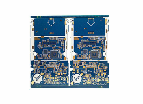
Circuit board to the board edge-stamp hole design
Generally, V-cut scoring or routing is used for the board design of circuit boards. In fact, in addition to these two designs, there is also a stamp hole design method.
The reason why it is called the "stamp hole" is because this PCB design is really the same as the full stamps we usually see. There are some small holes in the position of the board, which is convenient to use tools such as pliers to divide the board, or It is to directly break the connecting ribs between the small holes by hand to achieve the purpose of dividing the board.
The biggest advantage of the "stamp hole" splitting board is that it does not require any special splitting tools to achieve the purpose of splitting, unlike the other two methods that require special Scoring and routing machines. However, there are really many shortcomings of this stamp hole. The shortcomings are listed below:
▪ After the stamp hole is divided into the board, it is easy to leave burrs and board edges that are uneven. These burrs will sometimes cause assembly troubles. For example, the place where the display is located must not have easy contaminants such as burrs. These uneven board edges sometimes cause assembly interference and even cause functional problems.
▪ Regular splitting tools are usually not used to split the stamp hole. If the force is not applied properly during splitting, it is easy to bend the circuit board, causing solder cracks on the circuit board, or parts cracking... and other quality problems.

▪ Because of the uncertainty of the stamp hole splitting tool, the manufacturing process cannot be stable, and the PCB quality is difficult to control.
This kind of stamp hole is usually designed to be used on some circuit boards that cannot use V-cut as a sub-board, because V-cut has some limitations in its use. If the cut board is poorly designed, it will be unable to bear the weight and deform. So in the end, we still have to return to the stamp hole design, and the design of the stamp hole is also asked by some universities. If the design is not good, not only will it easily cause burrs to affect the assembly, sometimes additional processing is required, which is time-consuming, labor-intensive, and laborious. Not pleased.
The following are two different stamp hole designs. Can you see the difference? The same is the design of 5 small 1.0mm diameter stamp holes, but the result is very different. The PCB of the bad stamp hole design causes residues after the board is divided. The burrs protrude beyond the molding line. For precision products, most of these burrs require extra manpower for post-processing and smoothing. This not only wastes manpower but also wastes man-hours, increases costs, and the dust during grinding may also be contaminated. other products.
The difference between the two stamp hole designs is basically only in the design position of the ribs. The edges of the ribs of the better stamp hole design just fall in the middle of the stamp holes on the two sides, so that the stamp holes on the two sides are pre-formed. Hole, not only is it easier to break the edge of the board, it is also less likely that there will be burrs beyond the molding line after the edge of the board is broken.
Poorly designed circuit board [stamp hole]
The stamp hole is poorly designed, and the burrs of the protruding points generated after the board splitting exceed the molding line, and manual post-processing is required for smoothing, which not only wastes manpower but also wastes man-hours and increases costs. The scraps during the grinding may also contaminate other products. (The photo on the left seems to be a three-hole stamp hole design, but the result is the same)
Poor design of the stamp hole. After the board is divided, the burrs of the prominent points are beyond the molding line, and manual post-processing is required for smoothing, which not only wastes manpower but also wastes man-hours, and increases the cost. The thread requires manual post-processing and smoothing, which not only wastes manpower but also wastes man-hours and increases costs. The scraps during the smoothing may also contaminate other products.
Better-designed circuit board [stamp hole]
The stamp hole design is better. Although there are burrs after the PCB board is divided, almost all the burrs can be leveled within the molding line, which will not cause assembly interference.
The stamp hole design is better. Although there are burrs after the board is divided, almost all the burrs can be leveled within the molding line without causing interference in assembly. The stamp hole design is better. Although there are burrs after the board is divided, almost all the burrs can be leveled within the molding line without causing interference in assembly.