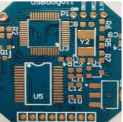
The various stages of the PCB assembly process include adding solder paste to the circuit board, component selection and placement, soldering, inspection and testing. All these processes are necessary and need to be monitored to ensure that the highest quality products are produced. The PCB assembly process described below assumes that surface mount components are being used, and almost all PCB assembly now uses surface mount technology.
Solder paste: Before adding components to the board, you need to add solder paste to the place where solder paste is needed on the board. These areas are usually component pads. This is achieved through a solder screen.
Solder paste is a paste formed by mixing small tin particles and flux. This can be deposited in place in one process, which is very similar to some printing processes.

Using a solder screen, place it directly on the circuit board and register it in the correct position. A runner moves through the screen, squeezing a small piece of solder paste through the hole on the screen and onto the circuit board. Since the tin screen is generated from the printed circuit board file, the tin screen has holes in the position of the tin pad, so that the solder is only deposited on the tin pad.
The amount of solder deposits must be controlled to ensure that the joints produced have the correct amount of solder.
Selection and placement: In this part of the assembly process, the board with solder paste then enters the selection and placement process. Here, a machine loaded with reels of components selects components from reels or other dispensers and places them in the correct positions on the circuit board.
The tension of the solder paste holds the components placed on the circuit board in place. This is enough to keep them in place, provided that the board is not shaken.
In some assembly processes, the pick-and-place machine will add small dots of glue to fix the components on the board. However, this is usually only done when the board is wave soldered. The disadvantage of this process is that any repair becomes more difficult due to the presence of glue, although some glues are designed to degrade during the welding process.
The position and component information required to design the pick-and-place machine comes from the design information of the PCB circuit board. This greatly simplifies pick and place programming.
Soldering: Once the component is added to the circuit board, the next stage of assembly, the production process is through its soldering machine. Although some boards may pass through a wave soldering machine, this process is not widely used for surface mount components these days. If wave soldering is used, no solder paste is added to the board because the solder is provided by the wave soldering machine. Reflow soldering technology is more widely used than wave soldering technology.
Inspection: After the circuit board passes through the soldering process, it is usually inspected. For surface mount boards using 100 or more components, manual inspection is not an option. On the contrary, automatic optical inspection is a more feasible solution. Existing machines are able to inspect boards and find bad joints, misplaced components, and in some cases, wrong components.
Test: Electronic products must be tested before they leave the factory. There are several ways to test them. More views on testing strategies and methods can be found in the "Test and Measurement" section of this website.
Feedback: In order to ensure the smooth operation of the manufacturing process, it is necessary to monitor the output. This is achieved by studying any faults detected. The ideal place is in the optical inspection stage, as this usually happens immediately after the welding stage. This means that process defects can be quickly detected and corrected before too many boards with the same problems are manufactured.
Summarize
In this overview, the PCB assembly process used to manufacture the loaded printed circuit board has been greatly simplified. PCB assembly and production processes are usually optimized to ensure very low defect levels and in this way produce the highest quality products. Given the number of components and solder joints in today's products, as well as the high requirements for quality, the operation of this process is critical to the success of the manufactured product.