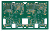
PCBA double-sided reflow soldering process (SMT) and precautions
At present, the mainstream circuit board assembly technology in the PCB industry should not be "full-board reflow soldering (Reflow)". Of course, there are other circuit board soldering methods, and this full-board reflow soldering can be divided into single-panel reflow soldering and Double-sided reflow soldering and single-sided reflow soldering boards are now rarely used, because double-sided reflow soldering can save space on the circuit board, which means that the product can be made smaller, so most of the boards seen on the market are Double-sided reflow soldering process.
(Off-topic, if there is no space restriction, in fact, the single-panel process can save an SMT process. If you compare the material cost with the SMT man-hour cost, maybe the single-panel is more cost-effective.)
Because the "double-sided reflow soldering process" requires two reflow soldering, there are some process restrictions. The most common problem is that when the board goes to the second reflow oven, the parts on the first side will be affected by Falling due to gravity, especially when the board flows into the high temperature area of the furnace for reflow soldering. This article will explain the precautions for the placement of parts in the double-sided reflow soldering process:

(Another digression, why when the second side is passed through the reflow oven, most of the small parts that have been tinned on the first side will not be re-melted and fall down? Why do only the heavier parts fall?)
Which SMD parts should be put through the reflow oven on the first side?
Generally speaking, smaller parts are recommended to be placed on the first side through the reflow oven, because the deformation of the PCB will be smaller when the first side is passed through the reflow oven, and the precision of solder paste printing will be higher, so it is more suitable for placement. Small parts.
Secondly, the smaller parts will not be at risk of falling during the second pass through the reflow oven. Because the parts on the first side are placed directly on the bottom side of the circuit board when the second side is hit, when the board enters the high temperature area of reflow soldering, it is less likely to fall off the board due to excessive weight.
Third, the parts on the first panel must go through the reflow oven twice, so its temperature resistance must be able to withstand the temperature of two reflow soldering. General resistors and capacitors are usually required to pass the high temperature of reflow soldering at least three times. It is to meet the requirements that some boards may need to go through the reflow oven again due to maintenance.
Which SMD parts should be placed on the second side through the reflow oven? This should be the focus.
▪ Large components or heavier components should be placed on the second side of the furnace to avoid the risk of parts falling into the reflow oven during the furnace.
▪ LGA and BGA parts should be placed on the second side of the furnace as much as possible, so as to avoid unnecessary re-melting risks during the second furnace, so as to reduce the chance of empty/false soldering. If there are small BGA parts with fine feet, it is not ruled out that it is recommended to put them on the first side through the reflow oven.
Placing the BGA on the first side or the second side to pass the furnace has always been controversial. Although placing the second side can avoid the risk of remelting the tin, usually the PCB will deform more seriously when the second side is passed through the reflow oven. On the contrary, it will affect the quality of tin eating, so the working bear will say that the BGA of the fine foot can be considered on the first side. But conversely, if the PCB is severely deformed, it must be a big problem for the delicate parts to be placed on the second side, because the solder paste printing position and the amount of solder paste will become inaccurate, so the focus should be Think of a way to avoid PCB distortion instead of putting BGA on the first side because of distortion, right?
▪ Parts that cannot withstand high temperatures too many times should be placed on the second side of the reflow oven. This is to prevent parts from being damaged by too many high temperatures.
▪ PIH/PIP parts should also be placed on the second side of the furnace, unless the length of the solder feet does not exceed the thickness of the board, otherwise the feet protruding from the PCB surface will interfere with the steel plate on the second side. The steel plate printed on the surface solder paste cannot be flatly attached to the PCB, causing the solder paste printing abnormal problem to occur.
▪ Some components may use soldering inside, such as a network cable connector with LED lights. You must pay attention to the temperature resistance of this part to pass the reflow oven twice. If not, you must place it on the second side. Pieces.
Only the parts are placed on the second side of the reflow oven, which means that the circuit board has been baptized by the high temperature of the reflow oven. At this time, the circuit board has somewhat warped and deformed, that is to say, tin The printing volume and printing position of the paste will become more difficult to control, so it is easy to cause problems such as empty soldering or short circuit. Therefore, it is recommended that you do not place 0201 and fine feet (fine feet) on the second side of the furnace. pitch) parts, BGA should also try to choose a solder ball with a larger diameter.
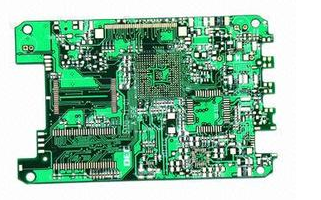
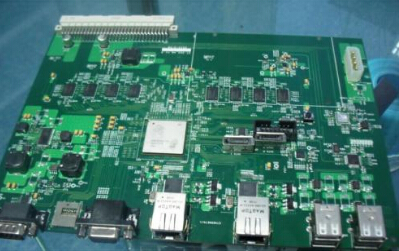
Refer to the pictures of the front and back sides of the SD card board at the top of the article, you should be able to clearly judge and point out which side will be arranged on the first side to pass parts through the reflow oven, and which side will be placed on the second Now it's over the oven!
In addition, in mass production, there are actually many methods of welding and assembling electronic parts on the circuit board, but each process is actually determined at the beginning of the circuit board design, because the circuit board The placement of the parts will directly affect the welding sequence and quality of the assembly, and the wiring will indirectly affect the assembly.
The current PCB soldering process can be roughly divided into full-board soldering and partial soldering. Full-board soldering is roughly divided into reflow soldering and wave soldering, while the local soldering of circuit boards includes carrier wave soldering. Soldering), selective soldering (Selective Soldering), non-contact laser soldering (Laser soldering), etc.