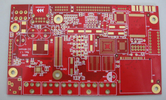
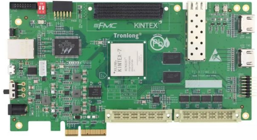
PCB is the basic electronic material in PCBA processing, and any PCBA processing is inseparable from PCB. How to accept the PCBA circuit board, and what are the acceptance standards that need to be paid attention to? How are these acceptance criteria evaluated?
Various characteristics can be observed on the PCB surface, the common ones are the following external characteristics and internal characteristics that cannot be observed from the surface. These PCBA appearance inspections are the main reference standards for circuit board acceptance.
1. Sheet edges and surface defects
▪ burr
▪ gap
▪ Scratches
▪ groove
▪ Fiber scratches
▪ Exposing fabrics and voids
▪ foreign inclusions
▪ White spots/microcracks
▪ Layered
▪ Pink circle
▪ Laminated void
2. Plated through holes
▪ The hole is misaligned
▪ foreign inclusions
▪ Plating or coating defects
3. Printed contact piece
▪ pit
▪ pinhole
▪ Nodulation
▪ exposed copper
4. Graphic size
▪ Size and thickness
▪ Aperture and graphics accuracy

▪ Wire width and spacing
▪ Coincidence
▪ Ring width
5. The flatness of the printed circuit board
▪ Bow
▪ distorted
One, PCB board edge
Defects such as burrs, nicks or halos may occur along the edge of the board, so certain acceptance requirements are required.
glitch
Burrs appear as small irregular lumps or bumps protruding from the surface and are the result of machining, such as drilling or cutting. Burrs can be divided into metallic burrs and non-metallic burrs.
▪ Ideal: The edge of the board is smooth, without burrs;
▪ Acceptable: the board edge is rough but does not damage the board edge;
▪ Rejection: The board edge is seriously damaged.
gap
▪ Ideal: smooth edges without gaps;
▪ Acceptable: Rough edges, but no defects. The depth of the notch is not more than 50% of the distance between the edge of the board and the nearest conductor or more than 2.5mm, whichever is less;
▪ Reject: Does not meet the standard.
Halo
Halo is a phenomenon of conductive fragmentation or delamination on or under the surface of the substrate caused by machining; halo usually appears as white areas around the hole or other machined parts, or both .
▪ Ideal: no halo;
▪ Acceptable: The range of the halo reduces the unaffected distance between the edge of the board and the nearest conductive pattern by no more than 50%, or more than 2.5mm, whichever is less;
▪ Reject: Does not meet the standard.
Laminated substrate
Laminate defects may be present when the printed circuit board manufacturer receives the printed circuit board substrate from the substrate manufacturer, or only become apparent during the manufacture of the printed circuit board.
Weave reveal, breakage and fiber breakage
▪ Exposure fabric: refers to a surface condition of the substrate, that is, the unbroken fabric fibers are not completely covered by the resin. Except for the area exposed to the fabric, the remaining distance between the conductors meets the minimum wire spacing requirement, then it is acceptable.
▪ Significant cloth pattern: refers to a surface condition of the substrate, that is, although the unbroken fabric fibers are completely covered by resin, the weave pattern is obvious. The visible cloth pattern is an acceptable condition, but the visible cloth pattern and the visible fabric sometimes have the same appearance, which is difficult to determine.
▪ Exposing fiber/fiber break: exposed fiber or fiber break does not cause the wire to bridge, and does not make the wire spacing below the minimum requirement, it can be accepted; if it causes wire bridging or the wire spacing is below the minimum requirement, it should be rejected .
Pits and holes
▪ Ideal: no pits and holes;
▪ Acceptable: pitting or voids shall not exceed 0.8mm (0.031in), and the affected area on each side shall be less than 5%. Pockmarks or voids did not cause bridging of conductors;
▪ Reject: Does not meet the standard.
Leukoplakia
White spots appear as discontinuous white squares or "cross" patterns under the surface of the substrate, and their formation is usually related to thermal stress. White spot is a phenomenon under the surface of the substrate, which occurs from time to time on new laminated substrates and on various boards made of fabric reinforced laminates. Since the white spots absolutely appear under the surface and are separated at the intersection of the fiber bundles, their appearance position is meaningless relative to the surface wires. The IPC-A-600G standard believes that white spots are acceptable for all products except for high-voltage applications as determined by the user, but it should be regarded as a process warning to remind the manufacturer that the process is on the verge of out of control.
Microcrack
▪ An internal condition in which the fibers in the laminated base material are separated. Microcracks can appear in fiber interweaving or along the length of fiber filaments. The microcrack condition is manifested as white dots or "cross patterns" connected under the surface of the substrate, which is usually related to mechanical stress.
▪ Micro-cracks reduce the wire spacing by no less than the minimum wire spacing value, and the micro-crack area does not exceed 50% of the distance between adjacent conductive patterns. The micro-cracks on the edge of the board do not reduce the minimum distance between the board edge and the conductive pattern (if not done According to regulations, it is 2.5mm), and the defects no longer expand after the thermal stress test, then the 2nd and 3rd grade boards can be accepted.
▪ If the diffusion of the micro-crack area exceeds 50% of the conductive pattern spacing, but the conductive pattern is not bridged, the level 1 board can be accepted (other conditions are the same as level 2 and 3).
Delamination and blistering
Delamination: The separation phenomenon that occurs between the layers in the substrate, between the substrate and the conductive foil, or any other printed circuit board layer.
Blistering: The phenomenon of local expansion and separation between any layers of the laminated substrate or between the substrate and the conductive foil or protective coating. The acceptance criteria are shown in Table 13-8. According to the relevant provisions of the IPC-A-600G standard, the acceptance conditions for Class 2 and 3 boards are as follows:
▪ The area affected by the defect does not exceed 1% of the area of each side of the board.
▪ The defect does not reduce the spacing between conductive patterns below the specified minimum spacing requirement.
▪ The blistering or delamination span is not more than 25% of the distance between adjacent conductive patterns.
▪ The defect does not expand after the thermal stress test that simulates the manufacturing conditions.
▪ The distance from the edge of the board is not less than the specified minimum distance between the board edge and the conductive pattern; if not specified, it is greater than 2.5mm.
According to the relevant provisions of the IPC-A-600G standard, the receiving conditions for the level 1 board are as follows:
▪ The area affected by the defect cannot exceed 1% of the area of each side of the board.
▪ The blistering or delamination span is greater than 25% of the spacing between adjacent wires, but the spacing between conductive patterns is not reduced below the minimum spacing requirement.
▪ The defect does not expand after the thermal stress test that simulates the manufacturing conditions.
▪ The distance from the edge of the board is not less than the specified minimum distance between the board edge and the conductive pattern; if not specified, it is greater than 2.5mm.
Foreign inclusions
Foreign inclusions refer to metal or non-metallic particles trapped in insulating materials.
Foreign inclusions can be detected in substrate raw materials, prepreg materials (stage B), or manufactured multilayer PCBs. Foreign objects may be conductors or non-conductors, both of which are based on their size and location to determine whether to reject them.
Usually translucent inclusions in the board are acceptable, and opaque inclusions are acceptable under the following conditions:
▪ The distance between the inclusion and the nearest conductor is not less than 0.125mm.
▪ did not cause the distance between adjacent wires to be lower than the minimum required value, if there is no special instructions, it should not be less than 0.125mm.
▪ The electrical performance of the board is not affected.